Study on optical and structural properties of TiO2/SnO2 thin film for optical devices
DOI:
https://doi.org/10.61343/jcm.v2i02.65Keywords:
Thin film, E-Beam, XRD, UV-Vis, AFMAbstract
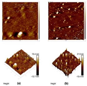
The TiO₂/SnO₂ thin films have garnered considerable attention for their application in optical devices due to their superior transparency and stability. This study investigates the optical and structural properties of TiO₂/SnO₂ thin films prepared through electron beam (e-beam) evaporation. The films were annealed at 400°C for one hour in a muffle furnace to evaluate the influence of annealing on their properties. Characterization techniques, including X-ray diffraction (XRD), UV-Vis spectroscopy, and atomic force microscopy (AFM), were employed to analyze the films. XRD analysis confirmed the presence of a distinct anatase TiO₂ phase with SnO₂ inclusions. Post-annealing, an enhancement in the peak intensities of both phases was observed, signifying improved crystallinity and atomic ordering. UV-Vis spectroscopy revealed that the annealed films exhibited reduced optical absorbance compared to their pristine counterparts. Furthermore, the optical bandgap increased from 4.10 eV for the pristine films to 4.32 eV after annealing. In AFM analysis 2D and 3D surface topographical images demonstrated that the annealed films show a smoother surface with reduced roughness, attributed to the enhanced crystallinity, which mitigates structural defects and grain boundary irregularities. These findings highlight the exceptional optical and structural characteristics of TiO₂/SnO₂ thin films, suggesting their potential for use in antireflective coatings, photodetectors, and waveguide structures in optoelectronic devices.
References
J Coronado, F Fresno, M Hernández-Alonso, R Portela, S Suárez, S García Rodríguez, and V de la Peña O'Shea. Design of Advanced Photocatalytic Materials for Energy and Environmental Applications. 2013.
M R D Khaki, M S Shafeeyan, A A A Raman, and W M A W Daud. J. Environ. Manag., 198:78–94, 2017.
V Kumaravel, S Mathew, J Bartlett, and S C Pillai. Appl. Catal. B Environ., 244:1021–1064, 2019.
H Tada, A Hattori, Y Tokihisa, K Imai, N Tohge, and S Ito. J. Phys. Chem. B, 104:4585–4587, 2000.
K Awa, R Akashi, A Akita, S ichi Naya, H Kobayashi, and H Tada. Chem. Phys. Chem., 20:2155–2161, 2019.
W Sangchay. Energy Procedia, 89:170–176, 2016.
A Kusior, L Zych, K Zakrzewska, and M Radecka. Appl. Surf. Sci., 471:973–985, 2019.
M Gülkı, Y Yılmaz, and T Aydogan. Appl. Surf. Sci., 554:149610, 2021.
M K Jangid, S Sharma, V P Meena, V P Arya, and S S Sharma. Evergreen, 11:178-185, 2024.
L Zhang, Y Wang, and H Zhao. Mater. Today Chem., 17:100303, 2020.
M K Jangid, S P Nehra, and M Singh. AIP Conf. Proc., 1393:311-312, 2011.
A Fujishima, K Honda, and S Kikuchi. Nature, 238:37–38, 1972.
C G Granqvist. Sol. Energy Mater. Sol. Cells, 91:1529–1598, 2007.
M K Jangid and M Singh. Int. J. Phys. Res., 2:15-23, 2012.
T Wågberg, P Johansson, and E Lindahl. Thin Solid Films, 539:114–121, 2013.
R Jafari, S Davari, and M Amjadi. J. Phys. D: Appl. Phys., 48:085303, 2015.
S Kumar, V Sharma, and P Singh. J. Mater. Sci.: Mater. Electron., 30:1675–1684, 2019.
J Lee, Y Kim, and H Park. ACS Appl. Mater. Interfaces, 10:175–185, 2018.
M K Jangid, S S Sharma, J Ray, D K Yadav, and C Lal. Int. J. Hydrogen Energy, 48:37921-37929, 2023.
P S Reddy, R Sharma, and K Ghosh. Ceram. Int., 46:16014–16021, 2020.
M K Jangid, S P Nehra, and M Singh. AIP Conf. Proc., 1349:685-686, 2011.
X Liu, J Wang, and L Chen. J. Mater. Sci., 42:640–645, 2007.
S Kumar, R Patel, and A Gupta. Thin Solid Films, 518:2795–2799, 2010.
F A Deorsola and D Vallauri. J. Mater. Sci., 43:3274–3278, 2008.
M M Miah, T Ahmed, and N Akhtar. J. Appl. Phys., 110:093510, 2011.
M Gharbi, R Karoui, and S Azzouz. J. Mater. Sci., 44:4312–4319, 2009.
S Shokri and M Parvin. Thin Solid Films, 520:5850–5854, 2012.
C Messaadi, T Ghrib, and J Jalali. J. Curr. Nanosci., 15:398–406, 2019.
G B Williamson and R C Smallman. Philos. Mag., 1:34–45, 1956.
B D Cullity. Elements of X-ray Diffraction. Addison-Wesley, London, 1978.
S Sakka. J. Non-Cryst. Solids, 100:227–239, 1988.
M K Jangid, S P Nehra, and M Singh. J. Nano-Electron. Phys., 3:460-468, 2011.
L Zhang, Y Li, and T Xu. J. Mater. Sci., 2021.
P Singh, A Mehta, and K Verma. Adv. Opt. Mater., 2020.
J Tauc. Mater. Res. Bull., 3:37–46, 1968.
A Fujishima and K Honda. Nature, 238:37–38, 1972.
M K Jangid, S S Sharma, J Ray, and S Jangid. Mater. Today: Proc., 67:847-851, 2022.
S Kumar, R Sharma, and M Gupta. J. Appl. Phys., 2022.
L Wang, H Zhang, and J Liu. Adv. Funct. Mater., 2021.
P Patra, S Mishra, and K Verma. Prog. Mater. Sci., 135:101073, 2023.
M K Jangid and S K Jangid. Trends Sci., 19:2067, 2022.
P Singh, A Sharma, and R Verma. J. Surf. Sci. Eng., 2021.
L Zhang, T Li, and H Xu. Adv. Thin Film Mater., 2022.
Downloads
Published
How to Cite
Issue
Section
Categories
License
Copyright (c) 2025 Ved Prakash Meena, S. S. Sharma, M. K. Jangid

This work is licensed under a Creative Commons Attribution 4.0 International License.
Copyright© by the author(s). Published by journal of Condensed Matter. This is an open access article distributed under the terms of the Creative Commons Attribution (CC BY) license (https://creativecommons.org/licenses/by/4.0/), which permits unrestricted use, distribution, and reproduction in any medium, provided the original author(s) and source are credited.