Quantum Transport Properties of Monolayer MoS2, WS2, and Black Phosphorus: A Comparative Study
DOI:
https://doi.org/10.61343/jcm.v1i02.20Keywords:
Transport properties, FET model, Transfer characteristics, Output characteristicsAbstract
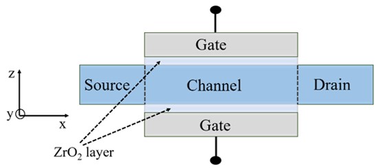
A comparative study of the performance analysis of dual-gate ballistic monolayer Molybdenum disulfide (MoS2), tungsten disulfide (WS2), and black phosphorus (BP) field-effect transistors (FETs) is presented. A thorough investigation of output and transfer characteristics infers that WS2 FET exhibits better performance as compared to MoS2 and BP. Furthermore, among all three FETs (MoS2, WS2, and BP), the WS2 based FET has a higher carrier velocity. However, variation of gate capacitance (CG) with gate voltage (VG) reflects a very good electrostatic gate control of MoS2 FET due to higher surface charge accumulation. Except for CG, the overall performance of WS2 based FET is better than MoS2 and BP.
References
K. S. Novoselov, A. K. Geim, S. V. Morozov, D.-e. Jiang, Y. Zhang, S. V. Dubonos, I. V. Grigorieva, and A. A. Firsov, “Electric field effect in atomically thin carbon films,” science 306, 666–669 (2004).
K. S. Novoselov, A. K. Geim, S. V. Morozov, D. Jiang, M. I. Katsnelson, I. V. Grigorieva, S. Dubonos, Firsov, and AA, “Two-dimensional gas of massless dirac fermions in graphene,” nature 438, 197–200 (2005).
A. C. Neto, F. Guinea, N. M. Peres, K. S. Novoselov, and A. K. Geim, “The electronic properties of graphene,” Reviews of modern physics 81, 109 (2009).
M. Y. Han, B. Özyilmaz, Y. Zhang, and P. Kim, “Energy band-gap engineering of graphene nanoribbons,” Physical review letters 98, 206805 (2007).
S. Pratap, S. Kumar, and R. P. Singh, “Certain aspects of quantum transport in zigzag graphene nanoribbons,” Frontiers in Physics 10, 940586 (2022).
S. Pratap, “Transport properties of zigzag graphene nanoribbons in the confined region of potential well,” Superlattices and Microstructures 100, 673–682 (2016).
S. Kumar, S. Pratap, V. Kumar, R. K. Mishra, J. S. Gwag, and B. Chakraborty, “Electronic, transport, magnetic, and optical properties of graphene nanoribbons and their optical sensing applications: A comprehensive review,” Luminescence (2022), doi.org/10.1002/bio.4334.
H. Zhang, M. Chhowalla, and Z. Liu, “2d nanomaterials: graphene and transition metal dichalcogenides,” Chemical Society Reviews 47, 3015–3017 (2018).
A. K. Geim and I. V. Grigorieva, “Van der waals heterostructures,” Nature 499, 419–425 (2013).
S. Pratap, N. Joshi, R. Trivedi, C. S. Rout, B. Chakraborty, et al., “Recent development of two-dimensional tantalum dichalcogenides and their applications,” Micro and Nanostructures, 207627 (2023).
B. Radisavljevic, A. Radenovic, J. Brivio, V. Giacometti, and A. Kis, “Single-layer mos2 transistors,” Nature nanotechnology 6, 147–150 (2011).
A. Kuc, N. Zibouche, and T. Heine, “Influence of quantum confinement on the electronic structure of the transition metal sulfide t s 2,” Physical review B 83, 245213 (2011).
A. Sebastian, R. Pendurthi, T. H. Choudhury, J. M. Redwing, and S. Das, “Benchmarking monolayer mos2 and ws2 field-effect transistors,” Nature communications 12, 693 (2021).
N. R. Glavin, R. Rao, V. Varshney, E. Bianco, A. Apte, A. Roy, E. Ringe, and P. M. Ajayan, “Emerging applications of elemental 2d materials,” Advanced Materials 32, 1904302 (2020).
L. Li, Y. Yu, G. J. Ye, Q. Ge, X. Ou, H. Wu, D. Feng, X. H. Chen, and Y. Zhang, “Black phosphorus field-effect transistors,” Nature nanotechnology 9, 372–377 (2014).
P. Bridgman, “Two new modifications of phosphorus.” Journal of the American chemical society 36, 1344–1363 (1914).
X. Ling, H. Wang, S. Huang, F. Xia, and M. S. Dresselhaus, “The renaissance of black phosphorus,” Proceedings of the National Academy of Sciences 112, 4523–4530 (2015).
H. Zhao, “Black phosphorus nanosheets: Synthesis and biomedical applications,” in Journal of Physics: Conference Series, Vol. 2566 (IOP Publishing, 2023) p. 012015.
S. Pratap and N. Sarkar, “Application of the density matrix formalism for obtaining the channel density of a dual gate nanoscale ultra-thin mosfet and its comparison with the semi-classical approach,” International Journal of Nanoscience 19, 2050010 (2020).
N. Yang, T. Wu, and J. Guo, “2dfet,” (2021), doi:10.21981/MCT5-1694.
K. Natori, “Ballistic metal-oxide-semiconductor field effect transistor,” Journal of applied Physics 76, 4879–4890 (1994).
F. Assad, Z. Ren, D. Vasileska, S. Datta, and M. Lundstrom, “On the performance limits for si mosfets: A theoretical study,” IEEE Transactions on Electron Devices 47, 232–240 (2000).
M. Lundstrom and J. Guo, “Nanoscale transistors: device physics, modeling and simulation”, (Springer Science & Business Media, 2006).
A. Rahman, J. Guo, S. Datta, and M. S. Lundstrom, “Theory of ballistic nanotransistors,” IEEE Transactions on Electron devices 50, 1853– 1864 (2003).
J. Wang, W. Liu, and C. Wang, “High-performance black phosphorus field-effect transistors with controllable channel orientation,” Advanced Electronic Materials 9, 2201126 (2023).
Downloads
Published
How to Cite
License
Copyright (c) 2023 Sandeep Kumar, Surender Pratap

This work is licensed under a Creative Commons Attribution 4.0 International License.
Copyright© by the author(s). Published by journal of Condensed Matter. This is an open access article distributed under the terms of the Creative Commons Attribution (CC BY) license (https://creativecommons.org/licenses/by/4.0/), which permits unrestricted use, distribution, and reproduction in any medium, provided the original author(s) and source are credited.