Synthesis of Multi Wall Carbon Nanotubes based Electronic Sensors for Internet of Things (IoT)
DOI:
https://doi.org/10.61343/jcm.v1i01.10Keywords:
Multiwall Carbon nanotubes, Internet of things (IOT), Chemical Vapour Deposition, Scanning Electron MicroscopeAbstract
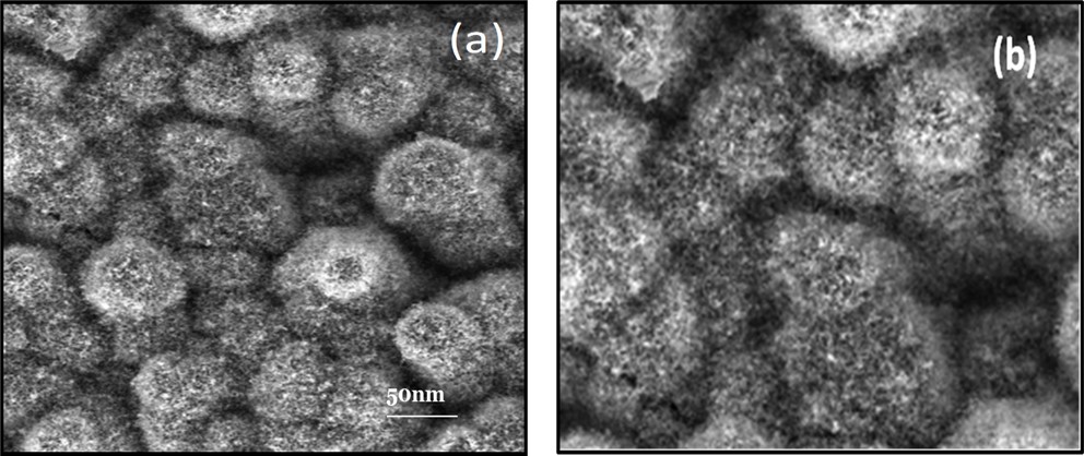
The Internet of Things (IoT) refers to advance devices other than computers that are connected to the Internet and can send and receive information. IoT is a new paradigm that has transformed traditional lifestyles into high-tech ones. It is the notion of a ubiquitous computer environment in which custom-sized electronics are effortlessly implanted into common things. Electronic sensors at the heart of the IoT detect physical/environmental occurrences, translate these measurements into electrical signals, and wirelessly transfer the data for remote computation. Indeed, the 5G communication and cloud computing stimulate the research in applications of carbon nanotubes in electronic devices. CNTs have demonstrated potential applications in electronics, biosensing, artificial intelligence and the Internet of ThingsIn present study, we report the synthesis of Multi Wall Carbon Nanotubes (MWCNTs) by Chemical Vapour Deposition (CVD) at 600C on Zinc Oxide (ZnO) catalyst coated silicon substrate by thermal evaporation technique. As-grown MWCNTs are characterized by Scanning Electron Microscope (SEM). High density growth of MWCNTs have been confirmed by SEM image. Catalyst nanoparticles play very important roles in the decomposition of the hydrocarbon source and to provide nucleation site for growth of MWCNTs. High MWCNT density is required for IoT-based sensors with high performance, sensitivity, selectivity, and distant sensing. Because IoT not only provides services but also creates massive amounts of data. Hence, this study would be helpful for the next generation 5G communication and cloud computing stimulate to enhance living style.
References
Applications of Carbon Nanotubes in the Internet of Things Era Jinbo Pang, Alicja Bachmatiuk, Feng Yang, Hong Liu, Weijia Zhou, Mark H. Rümmel, Gianaurelio Cuniberti, Nano-Micro Lett. (2021) 13:191
Y. Saitoa, S. Uemurab “Field emission from carbon nanotubes and its application to electron sources,” Carbon, vol. 38, pp. 169-182, Feb. 2000.
H. Dai, J. H. Hafner, A.G. Rinzler, D.T.Colbert, R.E. Smalley, “Nanotubes as nanoprobes in scanning probe microscopy,” Nature, vol. 384, pp. 147-150, Nov. 1996.
J.A. Cardenas, J.B. Andrews, S.G. Noyce, A.D. Franklin, Carbon nanotube electronics for IoT sensors. Nano Futures 4(1), 012001 (2020). https:// doi. org/ 10. 1088/ 239.
E. Amram Bengio, D. Senic, L.W. Taylor, D.E. Tsentalovich, P. Chen et al., High efficiency carbon nanotube thread antennas. Appl. Phys. Lett. 111(16), 163109 (2017)
R. Seelaboyina, S. Boddepalli, K. Noh, M. Jeon, W. Choi, “Enhanced field emission from aligned multistage carbon nanotube emitter arrays,” Nanotechnology, vol. 19, pp. 065605-4, May. 2008.
A. C. Eletskii, “Carbon nanotubes and their emission properties,” Phys.-Usp., vol. 45, pp. 369-402, April. 2002.
L. Wang, Z. Sun, T. Chen, W. Que, “Growth temperature effect on field emission properties of printable carbon nanotubes cathode,” Solid-State Electr., vol. 50, pp. 800-804, May. 2006.
S. Khan, Z. H. Khan, K.N. Tripathi, M. Husain, “Synthesis of carbon nanotubes using Ni95Ti5 nanocrystalline film as a catalyst,” J. Nanosci. Nanotechnol., vol. 7, pp. 1855-1859, June. 2007.
J. Ali, A. Kumar, S. Husain, M. Kumari, Harsh, M. Husain, “Characterization and field emission studies of uniformaly distributed multi-walled carbon nanotubes (MWMWCNTs) film grown by low pressure chemical vapour deposition (LPCVD),” Curr. Nanosci., vol. 7, pp. 333-336, June. 2011.
Z. H. Khan, S. Husain, M. Husain, “Variable range hopping in carbon nanotubes,” Curr. Nanosci., vol. 6, pp. 626-641, Dec. 2010.
S. Frank, P. Poncharal, Z. Wang, L. Walt, A. D. Heer, “Carbon nanotube quantum resistors.” Science., vol. 280, pp. 1744-1746, June. 1998.
V. Semet, V. T. Binh, P. Vincent, D. Guillot, K. B. K. Teo, M. Chhowalla, G. A.J. Amaratunga, W. I. Milne, P. Legagneux, D. Priba, “Field electron emission from individual carbon nanotubes of a vertically aligned array.” Appl. Phys. Lett., vol. 81, pp. 343-345, July. 2002.
J. F. AuBuchon, C. Daraio, L. H. Chen, A. I. Gapin, S. Jin, “Iron silicide root formation in carbon nanotubes grown by microwave PECVD”. J. Phys. Chem. B., vol. 109, pp. 24215-24219, Dec. 2005.
D. S. Chung, S. H. Park, H. W. Lee, J. H. Choi, S. N. Cha, J. W. Kim, J. E. Jang, K. W. Min, S. Cho, H. Yoon, M. J. Lee, J. S. Lee, C. K. Yoo, J. H. Kim, J. M. Jung, J. E. Y. W. Jin, Y. J. Park, J. B. You, “Carbon nanotube electron emitters with a gated structure using backside exposure processes,” Appl. Phys. Lett., vol. 80, pp. 4045-4047, May. 2002.
J. Ali, A. Kumar, S. Husain, M. Husain, “Effect of catalyst-deposition methods on the alignment of carbon nanotubes grown by low pressure chemical vapor deposition,” Nanosci. Nanotechnol. Lett., vol. 3, pp. 175-178, Aug. 2011.
S. Khan, K. N. Tripathi, M. Aggarwal, K. Tripathi, M. Husain, Z. H. Khan, “Field emission properties of Fe70Pt30 catalysed multiwalled carbon nanotubes,” J. Exp. Nanosci., vol. 2, pp. 215-228. April. 2007.
Downloads
Published
How to Cite
Issue
Section
License
Copyright (c) 2023 Muhammad Bilal, Shama Praveen

This work is licensed under a Creative Commons Attribution 4.0 International License.
Copyright© by the author(s). Published by journal of Condensed Matter. This is an open access article distributed under the terms of the Creative Commons Attribution (CC BY) license (https://creativecommons.org/licenses/by/4.0/), which permits unrestricted use, distribution, and reproduction in any medium, provided the original author(s) and source are credited.