E-ISSN:2583-9152

Research Article

Photonic Crystals

Journal of Condensed Matter

2024 Volume 2 Number 1 Jan-Jun
Publisherwww.thecmrs.in

Impact of Incident Angle on Defect Modes in Symmetric and Asymmetric One-Dimensional Photonic Crystals

Kumar V1*, Kumar R2
DOI:10.6134/jcm.v2i01.48

1* Vipin Kumar, Department Of Physics, Janta Vedic College, Baraut, UP, India.

2 Ravinder Kumar, Department of Physics, Janta Vedic College Baraut UP India2, Baraut, UP, India.

Our study has meticulously explored how the angle of incidence influences defect modes in one-dimensional photonic crystals (PCs) with a central defect. We focused on two types of PCs - those with symmetric and asymmetric configurations, each incorporating a single defect. In asymmetric PCs, we observed a unique defect mode occurring precisely at the central wavelength. In contrast, symmetric PCs displayed two separate defect modes near the central wavelength. We discovered that expanding the defect layer allows these two modes to converge into a unified central defect mode. It is important to note, though, that the intensities of these combined modes are distinct from those in asymmetric PCs. The transfer matrix method is employed to examine the propagation traits of the structures we proposed.

Keywords: Defects, Transfer matrix method, Transmittance

Corresponding Author How to Cite this Article To Browse
Vipin Kumar, , Department Of Physics, Janta Vedic College, Baraut, UP, India.
Email:
Kumar V, Kumar R, Impact of Incident Angle on Defect Modes in Symmetric and Asymmetric One-Dimensional Photonic Crystals. J.Con.Ma. 2024;2(1):6-10.
Available From
https://jcm.thecmrs.in/index.php/j/article/view/48

Manuscript Received Review Round 1 Review Round 2 Review Round 3 Accepted
2024-01-22 2024-01-16 2024-01-11 2024-01-06 2024-01-04
Conflict of Interest Funding Ethical Approval Plagiarism X-checker Note
None Nil Yes 20.98%

© 2024by Kumar V, Kumar Rand Published by Condensed Matter Research Society. This is an Open Access article licensed under a Creative Commons Attribution 4.0 International License https://creativecommons.org/licenses/by/4.0/ unported [CC BY 4.0].

Introduction

Since the pioneering work of Yablonovitch and John, the study of electromagnetic characteristics in photonic crystals – artificially engineered structures with periodic variations in dielectric constants – has been a focal point of research [1-17]. These studies have shown how periodic changes in dielectric functions significantly alter the spectral properties of electromagnetic waves. In such structures, the electromagnetic spectrum shows distinct allowed and forbidden bands of photonic energy, akin to the electronic bands in periodic potentials. This has led to the recognition of these materials, characterized by periodic dielectric modulation, as photonic band gap (PBG) materials [18]. Intriguingly, fundamental optical properties like band structure, reflectance, group velocity, and spontaneous emission rates can be manipulated by varying the dielectric function's spatial distribution [4, 5].

One-dimensional photonic crystals (1D PCs) are notable for their array of applications, such as dielectric mirrors, low-loss waveguides, optical switches, filters, and limiters. Both theoretical and experimental research confirms that 1D PCs possess absolute omnidirectional PBGs [19-23]. While pristine PCs are functional, doped or defective versions offer enhanced versatility. Semiconductor doping significantly broadens their application scope. The analogy between electromagnetism and solid-state physics has led to investigations into band structures in periodic materials and the emergence of localized modes within the band gap due to lattice defects. These doped photonic crystals show resonant transmission peaks within the band gap, indicative of localized states [24], resulting from changes in the interference patterns of incident waves. Modifications to introduce defects into pristine PCs include altering layer thicknesses [25], adding new dielectrics [26], or removing specific layers [27, 28].

The incorporation of defect states in photonic crystals, especially in two-dimensional (2D) and three-dimensional (3D) PCs, has attracted significant interest due to their vast applications. In 2D and 3D PCs, point defects can create microcavities, line defects can act as waveguides, and planar defects as perfect mirrors [29, 30]. Similarly, introducing defect layers in 1D PCs results in localized defect modes within the PBGs.

Given the easier fabrication of 1D PCs compared to their 2D and 3D counterparts, these defective modes can be efficiently integrated into 1D PCs for various applications, including optical filters and splitters, light-emitting diodes, and lasers [31-33].

In this communication, we focus on the theoretical analysis of defect mode properties in different materials, examining these defect modes using the transfer matrix method.

Theoretical Analysis

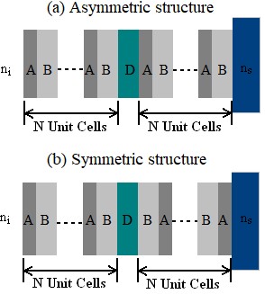
Figure 1 depicts a schematic diagram of a one-dimensional photonic crystal incorporating a defect.

jcm_48._01.jpg

Figure 1: Schematic diagram of 1-D Photonic crystal (a) Asymmetric structure (b) Symmetric structure.

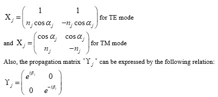
Our study examines two types of structures: asymmetric and symmetric, where 'H' and 'L' denote materials with high and low refractive indices, respectively. To determine the transmission spectrum, we utilize the transfer matrix method (TMM) [34]. Within this method, we can express the transfer matrix for each layer as follows:; jcm_48_02.jpg
In this context, 'j' represents either the H or L layers, and the terms Xj and Yj refer to the dynamical matrix and the propagation matrix,


respectively. The dynamical matrix for different polarizations can be defined by the following equations:
Where βj is called phase and can be expressed in terms of refractive index (ni), thickness of the layer (di) and wavelength (λ) of the incident wave as:jcm_48._04.jpg
For the two types of PCs considered in this study, the transfer matrix expressions can be written as:

The transmission coefficient, based on the matrix elements presented in equations (6 & 7), can be expressed as follows:
jcm_48._06.jpg

In this expression, δi,f is defined as ni,f(cosαj,f) for the TE polarized wave and as (cosαj,f)/ni,f for the TM polarized wave. Here, the subscripts 'i' and 'f' refer to the values in the medium of incidence and the medium of emergence, respectively. Meanwhile, the transmittance of the structure can be determined by the following:
jcm_48._07.jpg
In the following section, we will calculate the transmission spectra using equation (9), focusing on the photonic crystal with a defect as illustrated in Figure 1

Result and Discussion

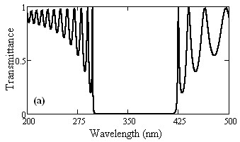
Consider a conventional photonic crystal denoted as "air/(AB)16/Substrate," known for its photonic band gap in the ultraviolet and visible regions. For this investigation, B is identified as TiO2, characterized by a refractive index (n) of 2.34867,

while A is represented by MgF2 with an n value of 1.3855. MgF2 is a particularly suitable material for photonic crystals due to its unique characteristics, including absorption commencing below 115nm and a refractive index close to unity. As the substrate, SiO2 (n=1.46) is employed. The thickness of layers A and B in Figure 1, adheres to the condition of the quarter-wavelength, specifically, nAdA=nBdB0/4, where λ0 designates the wavelength under consideration, set at 350nm for this study. Figure 2 illustrates the transmittance of this structure, as computed using Equation (9). It is evident from Figure 2 that a comprehensive band gap is present in the vicinity of the design wavelength, which is 350nm. The main objective of the present numerical computation is to introduce a defect in the middle of this structure, both symmetrically and asymmetrically, and subsequently investigate the defect modes in both configurations.

jcm_48._08.jpg

Figure 2: Transmission spectra of Air/(HL)16/SiO2 structure

Case 1: Symmetric Structure [Air/(HL)8D(HL)8/SiO2]

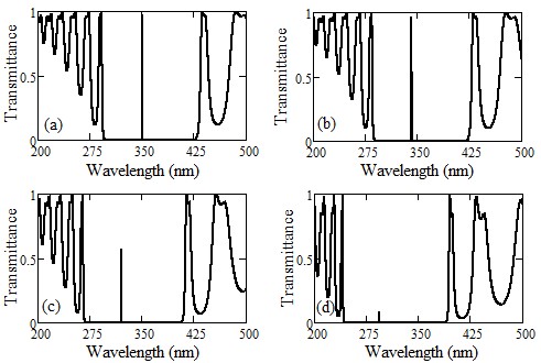
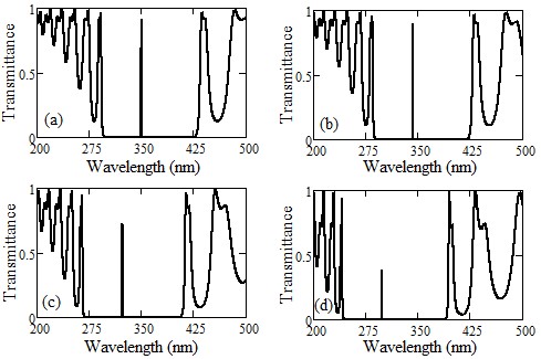
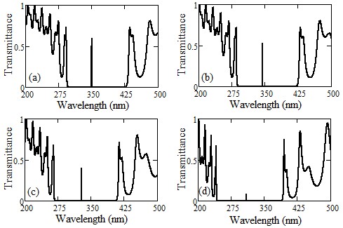
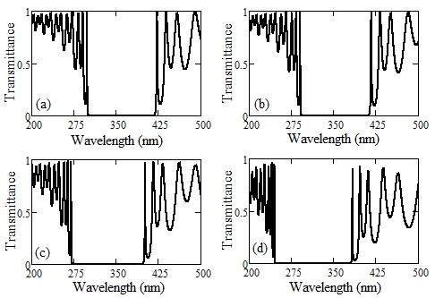
In the context of the asymmetric structure, we have presented transmission spectra for various defect materials, considering SiO2(n=1.46), Al2O3(n=1.66574), BGO(n=2.13), and ZnS(n=2.58789), at different angles of incidence (0º, 20º, 40º, & 60º). These transmission spectra are illustrated in Figures 3 to 6. Notably, these figures reveal a notable trend: as the angle of incidence increases, the defective modes gradually shift towards the lower boundary of the forbidden band gap. Furthermore, the intensity of these defect modes diminishes as the angle of incidence increases. It's worth noting that this decrease in intensity is particularly pronounced for defect materials with refractive indices that closely approach (nH-nL)/2.


jcm_48._09.jpg

Figure 3: Transmission spectra of Air/(HL)8D(HL)8/SiO2 structure for D=SiO2 @different incident angles (a) 0º (b) 20º (c) 40º (d) 60º.


jcm_48_10.jpg

Figure 4: Transmission spectra of Air/(HL)8D(HL)8/SiO2 structure for D=Al2O3 @different incident angles (a) 0º (b) 20º (c) 40º (d) 60º.


jcm_48_10.jpg

Figure 5: Transmission spectra of Air/(HL)8D(HL)8/SiO2 structure for D=BGO @different incident angles (a) 0º (b) 20º (c) 40º (d) 60º.


jcm_48_11.jpg

Figure 6: Transmission spectra of Air/(HL)8D(HL)8/SiO2 structure for D=ZnS @different incident angles (a) 0º (b) 20º (c) 40º (d) 60º

Case 2: Symmetric Structure [Air/(HL)8D(LH)8/SiO2]

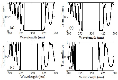
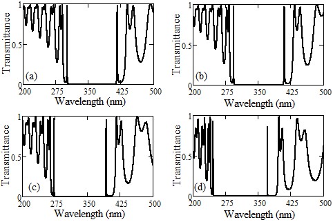
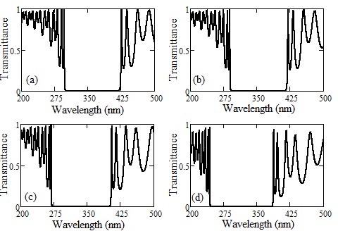
In the scenario of the symmetric structure, we have displayed transmission spectra for various defect layers, including SiO2, Al2O3, BGO, and ZnS, featuring a defect thickness of dD= λ0/4nD. These spectra are presented at different angles of incidence (0º, 20º, 40º and 60º) and are visualized in Figures 7-10.

These figures clearly show that in this configuration, two defect modes are noticeable near the edges of the photonic band gap (PBG) when the incidence angle is normal. As the angle of incidence increases, the defect mode on the left disappears, and the one on the right moves towards the left. Furthermore, as the refractive index of the defect layer increases, both defect modes gradually disappear. It's also observed that the intensity of these defect modes diminishes with a higher angle of incidence.

Notably, the behavior of these defect modes differs from the asymmetric case. These two defect modes essentially disappear when the material ZnS is employed, primarily because its refractive index closely approximates that of the H material. Therefore, by deliberately incorporating defects in a symmetric or asymmetric fashion, we can effectively create either one or two defect modes as needed. This approach allows for the tailored design and fabrication of photonic devices to meet specific requirements.


jcm_48_12.jpg

Figure 7: Transmission spectra of Air/(HL)8D(LH)8/SiO2 structure for D=SiO2 @different incident angles (a) 0º (b) 20º (c) 40º (d) 60º.

jcm_48_13.jpg

Figure 8: Transmission spectra of Air/(HL)8D(LH)8/SiO2 structure for D=Al2O3 @different incident angles (a) 0º (b) 20º (c) 40º (d) 60º.

jcm_48_14.jpg

Figure 9: Transmission spectra of Air/(HL)8D(LH)8/SiO2 structure for D=BGO @different incident angles (a) 0º (b) 20º (c) 40º (d) 60º.

jcm_48_15.jpg
Figure 10: Transmission spectra of Air/(HL)8D(LH)8/SiO2 structure for D=ZnS @different incident angles (a) 0º (b) 20º (c) 40º (d) 60º.

Conclusion

This research delves into the influence of the angle of incidence on defect modes within a one-dimensional photonic crystal (PC) that features a central defect. The investigation focuses on two distinct configurations of photonic crystals: symmetric and asymmetric. In the case of asymmetric PCs, we observe that a defect mode emerges exactly at the central wavelength. This is contrasted with symmetric PCs, where two separate defect modes are identified near the central wavelength. Interestingly, when the defect layer is expanded in symmetric PCs, these two defect modes coalesce into a singular mode at the central wavelength. However, it's important to note that the intensities of this merged mode differ significantly from those observed in the asymmetric PCs. This study not only contributes to a deeper understanding of the behavior of photonic crystals under varying conditions but also provides valuable insights that could be instrumental in the design and development of advanced photonic devices, where control over such defect modes is crucial for achieving desired optical properties and functionalities.

References

[1] E Yablonovitch. Phys. Rev. Lett., 58:2059, 1987.

[2] K M Ho, C T Chan and C M Soukoulis. Phys. Rev. Lett., 65:3152, 1990.

[3] J D Jonopoulos, P Villeneuve and S Fan. Nature, 386:143 1997.


[4] J A M Rojas, J Alpuente, J Pineiro and R Sanchez, Prog. Electromagn. Res., PIER 63:89 2006.

[5] E Yablonovitch and T J Gmitter, Phys. Rev. Lett., 63:1950 1989.

[6] J D Joannopoulos, R D Meade and J N Winn, Photonic Crystals: Molding the Flow of Light, Princeton Univ. Press, Princeton, NJ, 1995.

[7] E Burstein and C Weisbuch, Confined Electron and Photon: New Physics and Applications, Plenum Press, New York, 1995.

[8] G Du, X Zhou, C Pang, K Zhang, Y Zhao, G Lu, F Liu and A Wu, S. Akhmadaliev, S. Zhou et al., Adv. Opt. Mater., 8:2000426 2020.

[9] A K Goyal, A Kumar and Y Massoud, Crystals, 12:992 2022.

[10] A T Jervakani and B S Darki, Opt. Commun., 526:128884 2023.

[11] L Dan, D S Citrin and S Hu, Opt. Mater., 109:110256 2020.

[12] E Shahram, M Azardokht, K M Hossein, O Sareh, G Elham and H Mohsen, Photon. Netw. Commun., 31:516 2016.

[13] T Hiroya, T Isamu, F Hisayoshi and I Hideo, J. Lightwave Technol., 36(12):2517 2018.

[14] X Chen, H Ni, D Zhao and Y Wang, Appl. Opt., 61(26):7786-7792 2022.

[15] N Kumar, S Kaliramna and M Singh, Silicon, 14:6933 2022.

[16] N Kumar and J Saraf, Optik, 252:168577 2022.

[17] A Kumar, N Kumar and K B Thapa, Eur. Phys. J. Plus, 133:250 2018.

[18] C Soukoulis, Photonic Band Gap Materials, 71–79, Kluwer Academic, Dordrecht, 1996.

[19] J P Dowling, Science 282:1841 1998.

[20] E Yablonovitch, Opt. Lett. 23:1648 1998.

[21] D N Chigrin, A V Lavrinenko, D A Yarotsky andS V Gaponenko, Appl. Phys. A: Mater. Sci. Process. 68:25 1999.

[22] B Suthar, V Kumar, Kh S Singh and A Bhargava, Opt. Commun. 285(6):1505-1509 2012.

[23] V Kumar, Kh S Singh, S K Singh and S P Ojha, Prog. Electromagn. Res., PIER M 14:101-111 2010.

[24] G Guida, A de-Lustrac and P Priou, Prog. Electromagn. Res., PIER 41:1 2003.

[25] B Suthar and A Bhargava, IEEE: Photon. Tech. Lett., DOI:10.1109/LPT.2011.2178401.

[26] C M Soukoulis, Photonic band gaps and localization, NATO ARW, Plenum Press, New York, 1993.

[27] D R Smith, R Dalichaouch, N Kroll and S Schultz, J. Opt. Soc. Am., 10(2):314 1993.

[28] V Kumar, Kh S Singh and S P Ojha, Optik, 122:1183-1187 2011.

[29] J D Joannopoulos, R D Meade and J N Winn, Photonic Crystal: Molding Flow of Light, Princeton Univ. Press, Princeton, 1995.

[30] H Y Lee and T Yao, J. Appl. Phys., 93:819 2003.

[31] Z M Jiang, B Shi, D T Zhao, J Liu and X Wang, Appl. Phys. Lett., 79:3395 2001.

[32] M W Feise, I V Shadrivov and Y S Kivshar, Phys. Rev. E, 71:037602 2005.

[33] W D Zhou, J Sabarinathan, P Bhattacharya, B Kochman, E W Berg, P C Yu and S W Pang, IEEE: J. Quantum Electron, 37:1153 2001.

[34] P Yeh, Optical Waves in Layered Media, John Wiley and Sons, New York,1988.