E-ISSN:2583-9152

Review Article

Structural and Electrical Properties

Journal of Condensed Matter

2023 Volume 1 Number 2 Jul-Dec
Publisherwww.thecmrs.in

Preparation and effect of additives n-ZnO doped p-NiO Screen printed thick films on Structural and Electrical Properties

Mhaske U1*
DOI:10.61343/jcm.v1i02.25

1* Ujwala G Mhaske, Department Of Physics, Hpt Arts And Ryk Science College, Nashik, India.

ZnO doped NiO thick films preparation was effectively done using screen printing technique. Using characterisation techniques namely X-ray diffraction (XRD), scanning electron microscopy (SEM) & static gas sensing system, nanoparticles are synthesized. The structural properties of thick films were studied by XRD analysis and its result film shows polycrystalline nature of the films with a cubic structure and crystallite size found to be in the range of 182.1 to 354.4 A.U. SEM analysis of prepared films enabled the conclusion that the prepared films are uniform, large crystals and heavily agglomerated particles were observed spherical in shape. Also, with increase in concentration specific surface area increases. The quantitative chemical compositions were analysed by SEM-EDS and it shows nonstoichiometric in nature. The correlation between structural and morphological properties are reported. Electrical parameters of prepared thick films of ZnO doped NiO nanoparticles namely TCR, activation energy and sheet resistivity, specific surface area were analysed and evaluated at different concentration of zinc oxide. Electrical characterization results resistivity decreases from 6283.38 to 1972.73 Ω-cm with increase in wt.% concentration of ZnO; assured material has a semiconducting in nature. Such a prepared film can be used in fabrication of optoelectronic devices.

Keywords: ZnO, NiO, XRD, SEM-EDS, electrical resistivity, TCR, Activation energy

Corresponding Author How to Cite this Article To Browse
Ujwala G Mhaske, , Department Of Physics, Hpt Arts And Ryk Science College, Nashik, , India.
Email:
Mhaske U, Preparation and effect of additives n-ZnO doped p-NiO Screen printed thick films on Structural and Electrical Properties. J.Con.Ma. 2023;1(2):79-86.
Available From
https://jcm.thecmrs.in/index.php/j/article/view/25

Manuscript Received Review Round 1 Review Round 2 Review Round 3 Accepted
2023-11-02 2023-11-09 2023-11-16 2023-11-23 2023-12-01
Conflict of Interest Funding Ethical Approval Plagiarism X-checker Note
None Nil Yes 20.36

© 2023by Mhaske Uand Published by Condensed Matter Research Society. This is an Open Access article licensed under a Creative Commons Attribution 4.0 International License https://creativecommons.org/licenses/by/4.0/ unported [CC BY 4.0].

Introduction

Now a days nanocrystalline transition metal oxides TMOs have attracted extensive attention due to their various useful potential applications such as catalyst, TCO, photodetectors, gas sensors, photovoltaic devices, electrochemical supercapacitors, heat reflectors, solar cells and many opto- electronic devices [1-4]. One of the components in the Nickel-iron battery was NiO, so called as the Edison Battery, and is also a component in fuel cells. [5-7]. Nickel oxide (NiO) having low-cost material, chemical stability. Such NiO NPs possess typical characteristics mainly surface area-to-volume ratio high, low heat capacities, less porosity, large dispersion rates etc.

Nickel oxide is an antiferromagnetic p-type semiconductor metal oxide and exhibit NaCl-type cubic crystalline structure with lattice parameter (a= 4.816 A.U.); having bandgap ranges from 3.6 to 4.0 eV [8]. It can show different properties (optical, structural, and electrical etc.) on doping with foreign elements and these are important when materials selection and processing decisions are being made during the design of a device. As a results reduction particle size to nanometre scale shows more interesting properties in comparison with their bulk properties [9]. NiO nanoparticles have been characterized by using SEM, EDS, XRD, static gas sensing system.

Metal oxide thin and thick films have been prepared using various techniques namely spray pyrolysis, chemical vapor deposition, electrochemical deposition, sol-gel sputtering, screen printing technique, physical vapour deposition etc. such methods offer different advantages depending on the application of interest and many efforts have been conducted to obtain films with the desirable physical and chemical properties. Among all, screen-printing technique is relatively simple, inexpensive and its potential application for large area deposition make it very attractive and feasible for mass production processes.

 Recently zinc oxide (ZnO)is II-VI semiconductor material, has fascinated a great deal of attention because of its large exciton binding energy nearly (60 MeV) [10-11]. Due to numerous benefits over other oxides, films made of ZnO have now attracted a lot of attention in the development of optics or display devices [12-13]. ZnO has some

unique properties like non-toxic, inexpensive, with high light absorption and photoluminescence, low resistivity, direct band gap of 3.37 eV, excellent transparency in the visible region. Due to these unique properties, ZnO has been recognized as outstanding material for the optoelectronic devices as well as biosensor, gas sensors, photovoltaic panels, LEDs and optoelectronic are further expanded by its remarkable structural and morphologies of ZnO. As optical sensors, numerous ZnO morphologies, including nanoflakes and nanocomposites, have been synthesised and studied recently [14-15].

New applications in the field of material science, could be possible when the n-type SMO is combined with the p-type SMO.As compared to their single nano material, composite nanomaterials improve various characteristics significantly such as optical sensors performance [16-17].

With reference to other MOS ZnO inclusion in NiO improves the optical as well as electrical properties of the base material (NiO), both materials are extensively studied because of their potential optical applications [18-19]. Hence present work is carried out to study the impact of ZnO on the properties of NiO by preparation of mixed binary oxide ZnO-NiO thick film samples using SPT. Mainly structural, electrical properties of NiO-ZnO thick films are investigated in this paper. This study will give idea about preparation and their respective characterization for other TMOs.

Material, Method and Measurements

AR grade Nickel Oxide (NiO) and Zinc Oxide (ZnO) nano powders, acetone, B.C.A., ethyl cellulose etc. commercially available were used for preparation of screen-printed thick films. Structural and electrical characterization was done by using XRD technique, SEM and static gas sensing system.

Preparation of thick films of ZnO-NiO nanoparticles

Zinc oxide doped Nickel oxide thick film sensor was created by simple and standard screen-printing technique. It is a basic layer deposition and patterning process in thick film technology. Thixotropic paste was prepared by using 1 wt. %, 3 wt. %,5 wt. %,7wt % and 9 wt.


% of Zinc Oxide as an additive in Nickel Oxide; thick film was prepared by keeping 70:30 (inorganic to organic materials ratio). The inorganic part consists of nanoparticles of NiO and ZnO. The organic part consists of 8% ethyl cellulose (EC) and 92% butyl carbital acetate (BCA). All stoichiometric amounts of metal oxides and binders then mixed together into mortar and pestle and grind continuously for nearly 30 minutes. Then, a solution of BCA which was added drop wise into above crushed powder of metal oxide and binders. until proper thixotropic paste achieved. The prepared paste was then applied on previously cutted glass films with 1.5 X 2 cm dimensions. After complete coating of the films, these films were air dried firstly for 30 minutes followed by IR drying for 30 minutes. Finally, the prepared binary oxide film sensor was kept in muffle furnace for calcination process at temperature 400 ℃ nearly 2hours [20-21]. Now prepared thick films are ready for characterization [22-23].

Thick films Characterization: Characterization of prepared samples carried out by XRD, SEM with EDS and electrical characterization.

Thickness Measurement of the Films

Using weight difference method film thickness was calculated by equation (1) and its range observed from 60 to 68 μm

jcm_25_1.jpg              (1)

where,∆w = Weight difference of the film sensor before and after deposition, ρ = density of NiO = 6.67 gm/cm3 and ZnO =5.61 gm/cm3 and A= film area.

Result and Discussion

1. X-Ray diffraction (XRD) analysis

Crystallite size, lattice parameters, and crystallinity of prepared MBO NiO-ZnO thick film samples were investigated using X-ray diffraction. The films were scanned in the range between 20° and 80° and are compared to JCPDS data files.

jcm_25_2.jpg


jcm_25_3.jpg
jcm_25_4.jpg
jcm_25_5.jpg
jcm_25_6.jpg
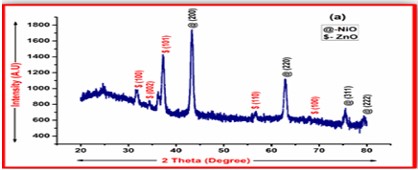
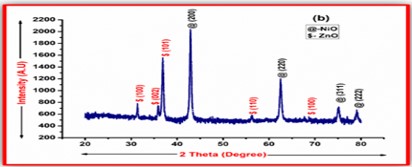
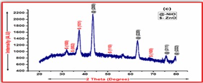
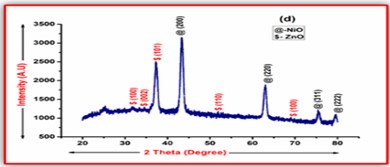
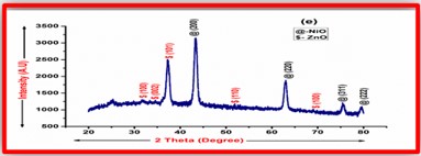
Figure 1: a,b,c,d,e represents XRD plots of Zn1,Zn3, Zn5, Zn7, Zn9 thick films respectively

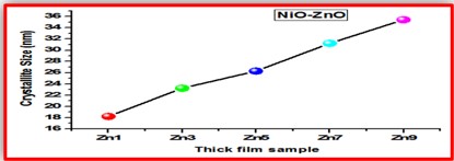
In Figure 1 (a-e) peaks of NiO denoted by @ and ZnO by $. All sample possess preferred orientation of NiO along (200) plane and matching with JCPDS File no. 01-075-0197 [24]. The ZnO crystal structure has found to be hexagonal wurtzite structure while Bunsenite face centered cubic (FCC) crystalline structure for NiO. For ZnO, preferential orientation along (101) peak according to the standard patterns (JCPDS file card no. 00-036-1451) [25]. Using Scherrer equation the crystallite size was determined. The crystallite size (D) of NiO-ZnO thick film samples was found to be 18.21 nm, 23.23 nm, 26.28 nm, 31.23 nm and 35.44 nm for Zn1, Zn3, Zn5, Zn7, and Zn9 samples respectively. It has been observed, as ZnO additive in wt.% increases, crystallite size of the films also increases. The rise in crystallite size indication is a significant factor of an optical sensor.  It may be due to the difference in atomic radii, Zn wt. % additive may increase the potential for crystallite agglomeration to increase in size of crystallite. [26]. A shear strength exists in the films as a result of the high defect formation, as evidenced by the observation of an increase in crystal size as well as a tiny


alteration in the lattice properties [27]. The variations in surface to volume ratios of produced films can be attributed for this behaviour.

Also, from figure 1 (a-e), it has been found with increase in concentration of additive, prominent peaks intensity also increases which tells the increase in the crystallinity of the prepared thick films. The increase in the crystallinity of films it could be the incorporation of ZnO or due to heterogeneous nucleation follows additive concentration placement in the lattice. Its width reduces as its intensity rises, indicating a bigger in crystallite size. These XRD patterns demonstrated good crystalline structure by having strong structural peaks. With increasing ZnO concentration, the crystallite size increases till it exceeds a maximum of 35.44 nm. The crystalline structure may be partially rebuilt as a result of the zinc anions at the ZnO sites replacing oxygen. This may be caused by the additive effects of the crystallization process [21, 28,29].

According to JCPDS card No. 01-075-0197, prominent peak of NiO located at 42.26°. According to obtained structural results, sample Zn9 exhibits the precise location of the prominent peak as well as the largest crystallite size. Sample Zn9 also exhibits good results when compared to other prepared thick film samples (Zn1-Zn7). The XRD results suggest that the MBO NiO-ZnO composed of crystalline NiO and ZnO nanostructures.

jcm_25_7.jpg
Figure 2: Crystallite size versus additive wt %.

The structural properties of thick NiO-ZnO films, including crystallite size, dislocation density, and micro strain has been measured and shown in table1. The microstrain of the thick film sample were calculated using Warren-Averbach method [30]. The intensity of the prominent peaks was improved and the FWHM found to be reduced as the ZnO wt.% additive increased, which reflects the improvement in crystallite size. The compatibility between variations in micro strain and dislocation density corresponding to alterations in additive in wt. % of ZnO is demonstrated in table 1. The table 1 shows as ZnO wt. % additive increased dislocation

density decreases and the grain size increases, which demonstrated how the ZnO additive affects grain size. The findings of this study were supported by reports by Amutha, C et. al. [31].

Table 1: Obtained values of dislocation density and micro strain of MBO films from XRD

SamplesDislocation density(n  x10-3Micro StrainƐ x10-3
Zn13.0155.377
Zn31.8534.267
Zn51.4483.713
Zn71.0253.138
Zn90.7962.757

2. SEM analysis

For investigation of surface morphology of the prepared MBO NiO-ZnO thick films FESEM apparatus [Model: SEM-JEOL JSM 6360 Model] was used.

jcm_25_8.jpg
jcm_25_9.jpg
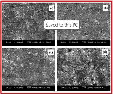
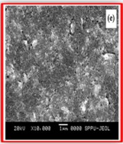
Figure 3: SEM micrographs of (a) Zn1, (b) Zn3, (c) Zn5, (d) Zn7, and (e) Zn9 MBO thick films at 10k magnification.

Figure 3 (a-e) depicts NiO-ZnO nanoparticles with a nearly spherical shape. The spherical nanoparticles are mixed with ZnO and distributed at randomly. FESEM images of NiO-ZnO thick films show that the surface of NiO-ZnO nanoparticles is uniform, fine, and has uncertain size distribution. Additionally, FESEM micrographs showed


a very porous structure. The accumulation of additive effects may lead to the formation of an extremely porous structure. Figure 3 (e) shows that some of the particles are heavily agglomerated and appear to be spherical in shape. The sample Zn9 show more voids as well as large grain size as compare to other samples. Small voids begin to occur when the sample's surface roughness and non - uniformity expand. The average particle size grows as a result of the concentration of wt. % ZnO additive increased. Furthermore, it was observed that the amount of Zn wt. % additive concentration increased, decreased the crystalline effect of NiO and irregularity was increased [17]. Zn1- Zn9 MBO NiO-ZnO thick film samples reveals agglomerated spherical morphology.

The all obtained outcomes from FESEM analysis of MBO NiO-ZnO thick films is tabulated in Table 2. From Table 2, it is clearly observed that as wt. % of ZnO additive increased the specific surface area of films also increased.

Table 2: Outcomes from FESEM

SampleDiameterd (nm)Sw (m2/gm)
Zn14152.171
Zn34022.248
Zn53023.003
Zn72184.173
Zn91247.359

3. Energy-dispersive X-ray spectroscopy (EDS) analysis

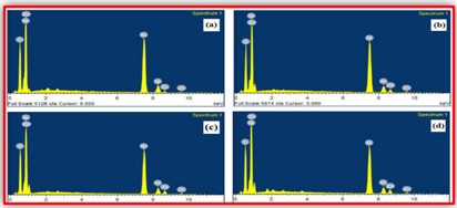
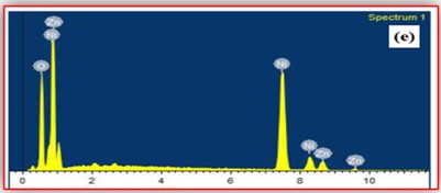
The elemental composition of prepared MBO NiO-ZnO thick films was determined using the spectra obtained by energy dispersive analysis of X-rays (EDS). EDS results reveals clearly peaks of Zn, Ni and O presence in Zn1, Zn3, Zn5, Zn7, and Zn9 samples in Figure 4 (a- e) respectively. From Figure 4 (a-e) it is clearly found that the wt. percentage of zinc oxide is increases with increasing additive in percentage. EDAX spectra shows the films have oxygen excess and also shows the Ni, Zn and O are non-stoichiometry [18-19] no any other elements in their structures. The variation of atomic and weight percentage of oxygen, nickel, and zinc determined by EDAX analysis are tabulated in table 3.

jcm_25_10.jpg


jcm_25_11.jpg
Figure 4: EDS spectra of (a) Zn1, (b) Zn3, (c) Zn5, (d) Zn7, and (e) Zn9 MBO thick films

Table 3: Elemental composition of MBO NiO- ZnO thick films

SampleElementsWeight %Atomic %
Zn1ONiZn39.4158.2502.3470.5628.4201.03
Zn3ONiZn39.2155.5105.2870.4927.1902.32
Zn5ONiZn40.2752.9106.8271.4525.5902.96
Zn7ONiZn40.5252.4307.0571.6725.2703.05
Zn9ONiZn38.9752.6008.4370.3825.8903.73

Crystallinity

Degree of structural order in a solid measured by crystallinity index Icry and it can be calculated through comparison of crystallite size obtained from XRD and SEM.

jcm_25_12.jpg      

where D_p is particle size by SEM, D by XRD using Debye Scherrer Formula from XRD and SEM, Icry is 21.013 for NiO-ZnO thick film.

For prepared sample, it is much more than 1 implies that the prepared thick films show polycrystalline type.

Electrical characterization of MBO NiO-ZnO thick films

According to literature survey, electrical properties like resistivity, mobility of charge carriers, conductivity, TCR and activation energy play a vital role in thick and thin film optical sensors. The prepared MBO NiO- ZnO (Zn1-Zn9) thick film samples is used to study impact of additives (ZnO) on NiO thick films was studied.

Resistivity

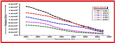
Using half bridge method, D.C. resistance of the films was measured in air atmosphere at 30 0 C to 350 0 C. The influence of additive or dopant (ZnO) on prepared NiO films is shown in Figure 7.6 (a-e). The Figure 7.6 (a), (b), (c), (d) and (e) plot shows resistance versus temperature for Zn1, Zn3, Zn5, Zn7, and Zn9 thick films of NiO-ZnO


samples respectively. From the Figure 5 (a-e) it has been found that in all sample cases the resistance has been decreases as surrounding temperature across the samples increased. These behaviours suggest the semiconducting nature of the all-thick film samples [32]. It is also observed that as wt. % ZnO additive increases in NiO the resistivity of the samples decreased, it may be the incorporation of ZnO in NiO which changes the lattice structure as well as reduced depletion layer. Resistivity of thick films decreases because of sufficient amount of NiO is present in compositional material. The ZnO particles are agglomerated around the NiO particles which would be forms the hetero p-n junction. The agglomeration of particle rises as wt. % additive increases [33-34]. The thickness of the films also shows linear variation, as additive increases the thickness of the samples decreased. The thickness of the Zn1, Zn3, Zn5, Zn7, and Zn9 thick films was obtained 68, 66, 65, 63, and 60 µm respectively.

jcm_25_13.jpg
Figure 5: Resistance vs temperature of (a) Zn1, (b) Zn3, (c) Zn5, (d) Zn7, and (e) Zn9 thick films

jcm_25_14.jpg
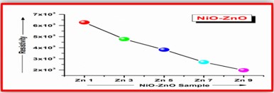
Figure 6: The variation in resistivity of MBO NiO-ZnO thick films

The resistivity of the samples found to be in the range of 6283.377 to 1972.727 Ω m. Figure 6 reveals the variation in resistivity of thick film samples with ZnO additive concentrations. According to obtained results of Chang et al., as crystallite size increases in response to an increase in the percentage of doping, conductivity also rises.

Activation Energy

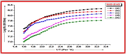
The activation energy is determined by using the Arrhenius equation from the obtained graph. By plotting logarithm of resistance against inverse temperature, the activation energy for low and high temperature regions was determined. Figure 7 (a-e)

depicts the electrical conductivity of samples of as a function of temperature and its inverse.

The energy gap between Fermi level and bottom of the conduction band is an electrical activation energy. As a result, the activation energy can be employed to determine Fermi level position [19]. The calculated values of activation energy for lower temperature region and higher temperature region for Zn1, Zn3, Zn5, Zn7, and Zn9 thick film samples was tabulated in Table 4.

jcm_25_15.jpg
Figure 7: Arrhenius plot of (a) Zn1, (b) Zn3, (c) Zn5, (d) Zn7, and (e) Zn9 thick films

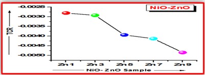
Temperature Coefficient of Resistance (T.C.R.)

The impact of wt. % additive (ZnO) inclusion in base material (NiO) is depicted in Figure 8. Figure 8 illustrates that the temperature coefficient is negative for all prepared MBO NiO-ZnO thick film samples.

jcm_25_16.jpg
Figure 8: TCR v/s wt. % additive of MBO NiO-ZnO thick films

Table 4: Electrical outcomes of MBO NiO- ZnO thick film samples

SampleResistivity(Ωm)Thickness(µm)TCR(/ °K)Activation Energy (eV)
At LTRAt HTR
Zn16283.37768-0.0028080.02260.1742
Zn34773.09366-0.0029260.01780.1536
Zn53823.93665-0.0039410.01370.1325
Zn72704.16963-0.0041330.01160.1185
Zn91972.72760-0.0048470.01010.1025

Conclusions

Using inexpensive, simple and powerful screen-printing technique, mixed binary oxides ZnO doped-NiO thick films with variation in a thickness deposition on glass substrates have been successfully done. The properties mainly


structural, morphological and electrical have been investigated step by step for ZnO doped NiO thick films. The deposited films annealed at 400℃. Annealed thick film XRD analysis shows a polycrystalline nature.  As film thickness of ZnO doped NiO films increased, crystallinity and morphological properties was also increased. Debye’s Scherrer equation was used for the average crystallite size calculation of most intense reflection (200) for NiO and (101) for ZnO. As wt.% additive increases defects obtained like dislocation density, micro strain also decreases. From SEM, it observed that few nanoparticles are in spherical shaped and most of them highly agglomerated. Surface area increases with increase in wt.% additives. EDS proved nonstoichiometric in nature from its quantitative elemental analysis of Ni, Zn and O. From electrical characterization, film resistance decreases with increase in concentration of ZnO it means ZnO-NiO thick films shows semiconducting behavior. Highly porous film shows high sensitivity, so such a prepared doped film can be useful in development of optical sensor.

Acknowledgement

The author (UMP) is very much thankful to working in department of Physics, Nashik. Author is gratefully acknowledged to SPPU Pune for providing facilities for film characterizations and its analysis.

Author Profile

Dr. Ujwala M. Pagar (Mhaske), currently working as Associate Professor in Physics at H.P.T. Arts and R.Y.K. Science College, Nashik 422005, (M.S.) India.

She has 14 years of teaching experience. Published 06 Research paper in Journal. Presented 3 papers in an international conference and attended several National and State level conferences.

References

1. M.A. Abbasi, Z.H. Ibupoto, A. Khan, O. Nur, M. Willander, Mater. Lett. 108, (2013)152.

2. M.D. Irwin, D.B. Buchholz, A.W. Hains, R.P.H. Chang, T.J. Marks, Proceedings of the National Academy of Sciences, art. No 0711990105, (2008)105.

3. J. Kim, J.-H. Yun, Y.C. Park, W.A. Anderson, Mater. Lett. 75, (2012) 99.

4. M.-J. Park, J.-Y. Jung, S.-M. Shin, J.-W. Song, Y.-H. Nam, D.-H. Kim, Thin Solid Films 599, (2016) 54.

5. K.C. Wang, P.S. Shen, M.H. Li, S. Chen, M.W. Lin, P. Chen, ACS Appl. Mater. Interfaces 6(15), (2014)11581.

6. J.H. Yun, J. Kim, Y.C. Park, S.J. Moon, W.A. Anderson, Thin Solid Films 547, (2013) 17.

7. S. Ahn, A.H. Tuan, S. Kim, C. Park, C. Shin, Y.J. Lee, Mater. Lett. 132, (2014) 06.

8. D. Zaouk, Y. Zaatar, R. Asmar, Microelectron. J. 37, (2006) 5.

9. A.A. Al-Ghamdi, W.E. Mahmoud, J. Yaghmour, F.M. AlMarzouki, J. Alloy. Compd. 486, (2009) 1

10. C. Kittel, Introduction to Solid State Physics. New York: Wiley, 1986.

11. R. J. Powell and W. E. Spicer, “Optical properties of NiO and CoO,” Phys. Review B, vol. 2, no. 6, pp. 2182– 2193, Sep. 15, 1970.

12. T. Satoh, N. P. Duong, and M. Fiebig, “Coherent control of antiferromagnetism in NiO”, Physical Review B 74 (1), 012-404, 2006.

13. L. Yuan, Z. P. Guo, K.Konstantinov, P. Munroe, and H. K. Liu, “Spherical clusters of NiO nanoshafts for lithium-ion battery anodes”, Electrochemical and solid-state letters 9 (11), A524-A528,2006

14. J. A. Dirksen, K. Duval, and T. Ring, “NiO thin film formaldahyde gas sensor,” Sens. Actuators B, vol. 80, pp. 106–115, 2001

15. C. R. Makkus, K. Hemmes, and J. H. W. Dewit, "A comparative-study of NiO(LI), LiFeO2, and LiCOO2 porous cathodes for molten-carbonate fuel-cells", Journal of the Electrochemical Society, 141(12), , pp. 3429-34381994, 1994.

16. M. N. Rumyantseva, L. I. Ryabova, T. A. Kuznetsova, M. Labeau, G. Delabouglise, A. M. Gas’Kov, "Sensor properties of polycrystalline SnO2 films doped with Ni", Inorg Mater, 35(1), pp. 54-59, 1999.

17. Tian F, Liu Y, “Synthesis of p-type NiO/n-type ZnO heterostructure and its enhanced photocatalytic activity”, Scripta Mater., 2013, 69, 417–419


18. Namseok Park, Ke Sun, Zhelin Sun, Yi Jinga and Deli Wang, “High efficiency NiO/ZnO heterojunction UV photodiode by sol–gel processing”, J. Mater. Chem. C, 1, pp. 7333-7338, 2013.

19. Xiaoyan Cai, Yun Cai, Yongjun Liu, He Li, Fei Zhang,Yude Wang, “High efficiency NiO/ZnO heterojunction UV photodiode by sol–gel processing, Journal of Materials Chemistry, C 44(1), pp 1-5, 2013.

20. Patil et. al., “Synthesis, characterization and gas sensing performance of SnO2 thin Films prepared by spray pyrolysis”, Bull Mater Sci, 2011; 34(1): 1–9.

21. Hazaa S Q, et. al. “Undoped and Cobalt Doped ZnO Thin Films Ethanol Gas Sensors”, Int Journal of Latest Res in Eng and Tech, 2016; 02 (08):01-05.

22. Mirzaei A et. al., “Fe2O3/Co3O4 composite nanoparticle ethanol sensor”, Kor Journal of Physical Society, 2016; 69 (3), 373–8.

23. U.J. Tupe, M. S. Zambare, A.V. Patil and P. B. Koli, “The Binary Oxide NiO-CuO Nanocomposite Based Thick Film Sensor for the Acute Detection of Hydrogen Sulphide Gas Vapours”, ISSN: 0973-3469, Vol.17, No. (3) 2020, Pg. 260-269.

24. B.D. Cullity, Elements of X-ray diffraction (Addison -Wesley) P102(1970) 102.

25. Dnyaneshwar, R. et al., (2017). “Photocatalytic degradation of dyes in water by analytical reagent grades ZnO, TiO2 and SnO2: a comparative study”, Drink. Water Eng. Sci., 10: 109-117.

26. Hindawi Journal of Nanomaterials Rafia Barir, Boubaker Benhaoua, Soufiane Benhamida, Achour Rahal, Toufik Sahraoui, and Rachid Gheriani5204639, “Effect of Precursor Concentration on Structural Optical and Electrical Properties of NiO Thin Films Prepared by Spray Pyrolysis”, Volume 2017, Article ID 5204639, 10 pages.

27. Chouaieb Zaouche, Yacine Aoun, Said Benramache, Abdelouahab Gahtar, “Synthesis and Characterization Of Deposited NiO Thin Films By Spray Pyrolysis Technique”, The Scientific Bulletin Of Valahia University - Materials And Mechanics –Vol. 17, No. 17 Doi 10.2478/Bsmm-2019-0015 27-32

28. Ukoba, K.O., Eloka-Eboka, A.C., Inambao, F.L, “Review of nanostructured NiO thin film deposition using the spray pyrolysis technique”, Renewable and Sustainable Energy Reviews, 82 (2018) 2900-2915.

29. B. Ramasubba Reddy, G. S. Harish, Ch. Seshendra Reddy, P. Sreedhara Reddy, “Synthesis and characterization of Cu doped NiO nanoparticles”, IJMER | ISSN: 2249–6645 | www.ijmer.com | Vol. 4 (2014) 62-66

30. K. Sankarasubramanian, P. Soundarrajan, T. Logu, S. Kiruthika, K. Sethuraman,R.R. Babu, K. Ramamurthi, “Influence of Mn doping on structural, optical and electrical properties of CdO thin films prepared by cost effective spray pyrolysis method”, Mater. Sci. Semicond. Process. 26 (2014) 346.

31. M. Ghougali O. Belahssen, A. Chala Structural, “Optical and Electrical Properties of NiO Nanostructure Thin Film”, J. NANO- ELECTRON. PHYS. 8, (2016) 040591-4

32. S.K. Noukelag b,c, H.E.A. Mohamed a,b , B. Moussa a,b , L.C. Razanamahandry d , S.K.O. Ntwampe e,f , C.J. Arendse, “Structural and optical investigations of biosynthesized bunsenite NiO nanoparticles (NPs) via an aqueous extract of Rosmarinus officinalis (rosemary) leaves”, 2214-7853/ 2020 Elsevier Ltd 1-5

33. P. A. Sheena, K.P. Priyanka, N. Aloysius Sabu, Boby Sabu, Thomas Varghese, Nanosystems: physics, chemistry, mathematics, 5 (3) (2014) 441-449.

34. M. P. Deshpande, Kiran N. Patel, Vivek P. Gujarati, Kamakshi Patel, S. H. Chaki, “Structural, Thermal and Optical Properties of Nickel Oxide (NiO) Nanoparticles Synthesized by Chemical Precipitation Method”, Advanced Materials Research Online: 2016-08-26 ISSN: 1662-8985, Vol. 1141, pp 65-71.