E-ISSN:2583-9152

Research Article

Quantum Transport Properties

Journal of Condensed Matter

2023 Volume 1 Number 2 Jul-Dec
Publisherwww.thecmrs.in

Quantum Transport Properties of Monolayer MoS2, WS2, and Black Phosphorus: A Comparative Study

Kumara S1, Pratap S2*
DOI:10.61343/jcm.v1i02.20

1 Sandeep Kumara, Department Of Physics Astronomical Science, Central University Of Himachal Pradesh, 176206, HP, India.

2* Surender Pratap, Department Of Physics Astronomical Science, Central University Of Himachal Pradesh, 176206, Hp, India.

A comparative study of the performance analysis of dual-gate ballistic monolayer Molybdenum disulfide (MoS2), tungsten disulfide (WS2), and black phosphorus (BP) field-effect transistors (FETs) is presented. A thorough investigation of output and transfer characteristics infers that WS2 FET exhibits better performance as compared to MoS2 and BP. Furthermore, among all three FETs (MoS2, WS2, and BP), the WS2 based FET has a higher carrier velocity. However, variation of gate capacitance (CG) with gate voltage (VG) reflects a very good electrostatic gate control of MoS2 FET due to higher surface charge accumulation. Except for CG, the overall performance of WS2 based FET is better than MoS2 and BP.

Keywords: Transport properties, FET model, Transfer characteristics, Output characteristics

Corresponding Author How to Cite this Article To Browse
Surender Pratap, , Department Of Physics Astronomical Science, Central University Of Himachal Pradesh, 176206, Hp, India.
Email:
Kumara S, Pratap S, Quantum Transport Properties of Monolayer MoS2, WS2, and Black Phosphorus: A Comparative Study. J.Con.Ma. 2023;1(2):94-98.
Available From
https://jcm.thecmrs.in/index.php/j/article/view/20

Manuscript Received Review Round 1 Review Round 2 Review Round 3 Accepted
2023-11-05 2023-11-12 2023-11-18 2023-11-24 2023-12-01
Conflict of Interest Funding Ethical Approval Plagiarism X-checker Note
None Nil Yes 20.96

© 2023by Kumara S, Pratap Sand Published by Condensed Matter Research Society. This is an Open Access article licensed under a Creative Commons Attribution 4.0 International License https://creativecommons.org/licenses/by/4.0/ unported [CC BY 4.0].

Introduction

In 2004 at the University of Manchester, synthesis of the first one atom thick layer of graphene was done by K. S. Novoselove et al. [1-2]. This discovery increases the interest of the scientific community in single-atom-thick two-dimensional (2D) materials to explore their basic properties and applications for device purposes. The absence of energy band gap in the single layer of graphene prevents to manipulate electronic devices made up of graphene [3-5]. A number of different methods are employed for the band gap engineering of graphene, for instance, cutting graphene into one-dimensional strips known as graphene nanoribbons [5-7]. However, these methods add complexity and reduce the charge carrier mobility. As a result of this, the scientific community has focused on other single or few-layered 2D materials. With inherent band gap, transition metal dichalcogenides (TMDs) have overcome the drawbacks of gapless graphene to become a potential material for FET applications in nanoelectronics [8]. Also, they can be easily exfoliated and are stable under vast conditions [9-10].

In the group of materials exhibiting semiconducting nature, TMDs structure is represented by MX2, where M stands for a transition metal atom (such as Mo or W) and X for a chalcogen atom (such as S, Se, or Te). TMDs feature a multilayer structure with transition metal atoms positioned in the middle of two chalcogen atoms’ hexagonal planes. TMDs have an overall hexagonal or rhombohedral symmetry, but the metal atoms inside them

jcm_20_1.jpg
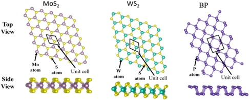
Figure 1: 2D Lattice structures of monolayer MoS2, WS2, and BP

display octahedral or trigonal prismatic coordination. According to the literature, MX2 has a band gap ranging from 1.1 to 2 eV [10]. Therefore, 2D monolayer semiconducting TMDs may be suited for applications that resemble complementary metal oxide-semiconductor (CMOS) logic devices and may be a possible substitute for silicon (Si). Similar to graphene, it is feasible to mechanically exfoliate

TMDs’ bulk crystals into atomically thin flakes. The exfoliation of 2D TMDs frequently involves electrochemical synthesis, ion intercalation, and mechanical cleavage techniques. Among all the techniques, for mass manufacturing of nanosheets or nanoflakes of layered TMDs, exfoliation via chemicals is most promising [10].

Monolayer MoS2 has an electron mobility comparable to that of graphene, but with nonzero band gap. The bulk and monolayer forms of MoS2 have indirect and direct band gaps, respectively. MoS2 exhibits a transition from 1.3 eV for the bulk indirect band gap to 1.8 eV for the monolayer direct band gap [11]. The reason of this band gap in monolayer MoS2 is the symmetry breaking of honeycomb lattice [10]. Additionally, monolayer WS2 with an energy band gap of 1.9 eV is anticipated to have a wide range of applications in energy conversion and renewable energy technologies [12]. Recently, Sebastian et al. explored the FET performance of experimentally synthesized monolayers of MoS2 and WS2 [13]. Moreover, elemental 2D layered materials such as silicene, phosphorene has been recognized as a new kind of material with unique properties that is critical to the application of electronics and optoelectronics [14]. Monolayer BP (known as “Phosphorene”) exhibits a puckered honeycomb structure because each phosphorus atom forms three covalent bonds with its nearest neighbours [15].

In 1914, Bridgman synthesized BP under high pressure and temperature, a brand-new 2D isomer of white phosphorus that is also the most stable allotrope of phosphorus at ambient temperature [16]. BP has received great scientific attention since the successful fabrication of few-layer phosphorene FET in 2014 [15]. BP also exhibits thickness dependent band gap ranging from 0.3 to 2 eV [17]. BP nanosheets, which are more favoured for spectroscopic and electrical studies, have recently been effectively synthesized using liquid-phase exfoliation and chemical vapor de position [18]. 2D lattice structures of monolayer MoS2, WS2, and BP are depicted in figure 1. In this work, a comparative study of the ballistic performance of dual-gate monolayer MoS2, WS2, and BP FETs is investigated. We have shown the variation of source to drain current density (IDS) against drain voltage (VD). Also, the gate control performances of monolayer MoS2, WS2, and BP FETs are explained by plotting


IDS against gate voltage (VG). Moreover, an explanation of the variation of the average velocity of carriers with VD and gate capacitance (CG) with VG is provided.

Simulation Method & Theoretical Formulation

jcm_20_2.jpg
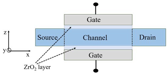
Figure 2: Schematic of ballistic n-type monolayer MoS2, WS2, and BP MOSFETs [19].

We have made a comparison between the ballistic performance of monolayer MoS2, WS2, and BP channel-based metal-oxide-semiconductor field-effect transistors (MOSFETs). The simulations have been performed on “2DFET” simulation tool [20]. This is a Python simulator for calculating the I-V characteristics of FETs based on 2D materials. The 2D FET channel can be either TMDs or BP. Using this simulator one can model the ballistic limit as well as transport with scattering of both n-type and p-type transistors [20]. The schematic of the structure used for simulation is shown in figure 2. Tables 1 and 2 show the input and control parameters used for simulation in the FET tool, respectively. The theoretical formulation for simulation is described below.

The performance of ballistic MOSFET model can be calculated analytically [21-23]. The equilibrium electron density (n0) at the top of the energy barrier with zero terminal bias is

jcm_20_3.jpg

where, E represents the energy, D(E) is the density of state at E, f is the Fermi distribution function, and EF is the Fermi energy. The biasing of the source and drain terminal modulates the energy barriers. Therefore, electrons from the source occupy the positive velocity states at the top of the barrier, while electrons from the drain fill the negative states. The electron density become

jcm_20_4.jpg

where EFS, EFD denotes the Fermi level in the source and drain, respectively. Uscf denotes the self-consistent surface potential, which is defined as

jcm_20_5.jpg

where C is the sum of the capacitances of the gate (CG ), source (CS), and drain (CD), i.e., C =CGVG + CDVD + CSVS. The difference between the flux from the source and the drain may be used to determine ballistic current (IDS) once convergence is achieved. Moreover, at the top of the barrier, the average velocity of carriers is given by

  jcm_20_6.jpg 

where q and N represent the electronic charge and density, respectively. For the detailed derivation of the proposed model, one can follow Ref. [24].

Table 1: Parameters taken for the simulation of IDS versus VD characteristics of FET in ballistic regime.

Gate lengthGate voltage (VG)Thickness of insulator (tins)Dielectric constant of insulator (εr)Drain voltage (VD)
20 nm 0- 0.6V3 nm29 (ZrO2) 0- 0.6V

Table 2: Control parameters for the device model.

Threshold voltage (VT)Gate control parameter (αG) = CG/CDrain control parameter (αD) = CD/CTemperature (T)
0.3 V0.90.03 300 K

Results and Discussion

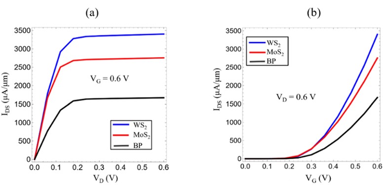
We have chosen the x-direction along the transistor channel and IDS versus VD output characteristics of dual gate MOSFETs with high dielectric (ZrO2) insulator of thickness (tins) 3 nm is shown in figure 3 (a). It is clear from figure 3 (a) that for an n-type MOSFET, under low bias (VG < VT), the device is off. Because at low VG the energy barrier between the source and drain is high, no current flows through the channel. At low VG, the high value of VD only lowers the energy of the carriers in the drain contact. However, the high value of VG reduces the energy barrier, i.e., electron flow from source to drain. For a fixed value of VG (VG > VT), the average velocity of charge carriers increases with the increase of VD and then saturates. As a result, IDS saturates at high VD. For low values of VD, the increase in the IDS linearly varies with an increase in the VG, i.e., the device behaves as the resistor. Among all three materials (MoS2, WS2, and BP), within the ballistic regime, output performance of WS2 transistor is best.


jcm_20_7.jpgFigure 3: Comparison of output characteristics of n-type monolayer MoS2, WS2, and BP FETs. (a) IDS versus VD at maximum VG = 0.6 V. (b) IDS versus VG at maximum VD = 0.6 V.
We increase the VG ranging from 0 to 0.6 V in the steps of approximately 0.06 V. As shown in figure 3 (b), for all FETs when VG > VT, IDS increases with VG. Although, for VD = 0.6V, WS2 has high value of IDS among all the FETs but all three FETs exhibit same value of ON-current. Moreover, except BP, MoS2 and WS2 show good gate electrostatic control and high values of IDS. Therefore, for future FETs, monolayer WS2 and MoS2 demonstrate huge potential to replace the silicon channel.

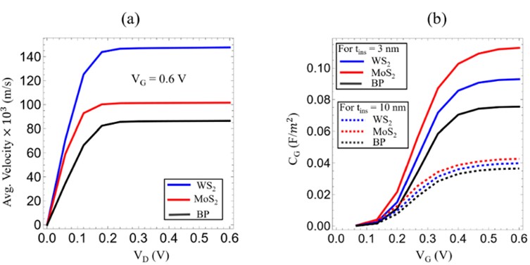
In figure 4 (a), for VG = 0.6 V, we plotted the average electron velocity versus VD. We observed that for VD < 0.2 V, all the materials show linear behaviour of electron velocities with increase in VD. This happens because with increase in the VD from 0 to 0.2 V, the source to drain voltage decreases, and it acquires a minimum value for VD > 0.2 V. Therefore, above 0.2 V, the electrons acquire their maximum average velocity. The different values of average velocities in different materials are attributed to their different electron effective masses. Previous studies show that BP has directional effective mass dependency for the electrons [25]. The lower value of average electron velocity of BP FET is due to the higher effective mass of electron in the chosen direction.

jcm_20_8.jpgFigure 4: For n-type monolayer MoS2, WS2, and BP FETs (a) ballistic transfer characteristics at maximum VD = 0.6 V and (b) variation of gate CG with increasing VG as a function of insulator thickness (tins).

Further, as shown in figure 4 (b), we observe the CG versus VG characteristics of the 2D FET with different materials (i.e., MoS2, WS2, and BP) and a 3 nm and 10 nm insulating layer. For both 3 nm and 10 nm insulating layers, MoS2 shows a higher value of CG than WS2 and BP. This happens because of the higher dielectric constant of MoS2 as compared to WS2 and BP. With a higher VG, the device is in the accumulation region, and as the VG decreases, the device comes into the depletion region. Therefore, a reduction in the CG is observed with a reduction in the VG. For tins = 3 nm, higher capacitances are observed for all materials (MoS2, WS2, and BP) as compared with tins = 10 nm because of the inverse dependency of thickness.

Conclusion

In conclusion, we observe that the output characteristics (IDS versus VD) of n-type MoS2, WS2, and BP FETs follow the same trend. For VG > VT, WS2 FET has a higher IDS as compared to MoS2 and BP. Transfer characteristics (IDS versus VG) show approximately the same value (≈ 0.2 V) of ON-current for all FETs with different values of maximum current. Also, for VG = 0.6 V, WS2 FET has higher average carrier velocity when plotted VD. The higher average velocity is due to the lower effective mass of carriers in WS2 than MoS2 and BP. Moreover, the higher value of CG for MoS2 FET is due to higher surface charge accumulation as compared to WS2 and BP based FETs. Therefore, except for CG, WS2 FET has better performance.

Acknowledgement

SK wishes to acknowledge UGC- New Delhi for financial support during research in the form of UGC- Senior Research Fellowship (SRF). SP would like to express gratitude to the Department of Physics and Astronomical Science (CUHP) for providing the facility for this research.

References

1. K. S. Novoselov, A. K. Geim, S. V. Morozov, D.-e. Jiang, Y. Zhang, S. V. Dubonos, I. V. Grigorieva, and A. A. Firsov, “Electric field effect in atomically thin carbon films,” science 306, 666–669 (2004).

2. K. S. Novoselov, A. K. Geim, S. V. Morozov, D. Jiang, M. I. Katsnelson, I. V. Grigorieva, S. Dubonos, Firsov, and AA, “Two-dimensional


gas of massless dirac fermions in graphene,” nature 438, 197–200 (2005).

3. A. C. Neto, F. Guinea, N. M. Peres, K. S. Novoselov, and A. K. Geim, “The electronic properties of graphene,” Reviews of modern physics 81, 109 (2009).

4. M. Y. Han, B. Özyilmaz, Y. Zhang, and P. Kim, “Energy band-gap engineering of graphene nanoribbons,” Physical review letters 98, 206805 (2007).

5. S. Pratap, S. Kumar, and R. P. Singh, “Certain aspects of quantum transport in zigzag graphene nanoribbons,” Frontiers in Physics 10, 940586 (2022).

6. S. Pratap, “Transport properties of zigzag graphene nanoribbons in the confined region of potential well,” Superlattices and Microstructures 100, 673–682 (2016).

7. S. Kumar, S. Pratap, V. Kumar, R. K. Mishra, J. S. Gwag, and B. Chakraborty, “Electronic, transport, magnetic, and optical properties of graphene nanoribbons and their optical sensing applications: A comprehensive review,” Luminescence (2022), doi.org/10.1002/bio.4334.

8. H. Zhang, M. Chhowalla, and Z. Liu, “2d nanomaterials: graphene and transition metal dichalcogenides,” Chemical Society Reviews 47, 3015–3017 (2018).

9. A. K. Geim and I. V. Grigorieva, “Van der waals heterostructures,” Nature 499, 419–425 (2013).

10. S. Pratap, N. Joshi, R. Trivedi, C. S. Rout, B. Chakraborty, et al., “Recent development of two-dimensional tantalum dichalcogenides and their applications,” Micro and Nanostructures, 207627 (2023).

11. B. Radisavljevic, A. Radenovic, J. Brivio, V. Giacometti, and A. Kis, “Single-layer mos2 transistors,” Nature nanotechnology 6, 147–150 (2011).

12. A. Kuc, N. Zibouche, and T. Heine, “Influence of quantum confinement on the electronic structure of the transition metal sulfide t s 2,” Physical review B 83, 245213 (2011).

13. A. Sebastian, R. Pendurthi, T. H. Choudhury, J. M. Redwing, and S. Das, “Benchmarking monolayer mos2 and ws2 field-effect transistors,” Nature communications 12, 693 (2021).

14. N. R. Glavin, R. Rao, V. Varshney, E. Bianco, A. Apte, A. Roy, E. Ringe, and P. M. Ajayan, “Emerging applications of elemental 2d materials,” Advanced Materials 32, 1904302 (2020).

15. L. Li, Y. Yu, G. J. Ye, Q. Ge, X. Ou, H. Wu, D. Feng, X. H. Chen, and Y. Zhang, “Black phosphorus field-effect transistors,” Nature nanotechnology 9, 372–377 (2014).

16. P. Bridgman, “Two new modifications of phosphorus.” Journal of the American chemical society 36, 1344–1363 (1914).

17. X. Ling, H. Wang, S. Huang, F. Xia, and M. S. Dresselhaus, “The renaissance of black phosphorus,” Proceedings of the National Academy of Sciences 112, 4523–4530 (2015).

18. H. Zhao, “Black phosphorus nanosheets: Synthesis and biomedical applications,” in Journal of Physics: Conference Series, Vol. 2566 (IOP Publishing, 2023) p. 012015.

19. S. Pratap and N. Sarkar, “Application of the density matrix formalism for obtaining the channel density of a dual gate nanoscale ultra-thin mosfet and its comparison with the semi-classical approach,” International Journal of Nanoscience 19, 2050010 (2020).

20. N. Yang, T. Wu, and J. Guo, “2dfet,” (2021), doi:10.21981/MCT5-1694.

21. K. Natori, “Ballistic metal-oxide-semiconductor field effect transistor,” Journal of applied Physics 76, 4879–4890 (1994).

22. F. Assad, Z. Ren, D. Vasileska, S. Datta, and M. Lundstrom, “On the performance limits for si mosfets: A theoretical study,” IEEE Transactions on Electron Devices 47, 232–240 (2000).

23. M. Lundstrom and J. Guo, “Nanoscale transistors: device physics, modeling and simulation”, (Springer Science & Business Media, 2006).

24. A. Rahman, J. Guo, S. Datta, and M. S. Lundstrom, “Theory of ballistic nanotransistors,” IEEE Transactions on Electron devices 50, 1853– 1864 (2003).

25. J. Wang, W. Liu, and C. Wang, “High-performance black phosphorus field-effect transistors with controllable channel orientation,” Advanced Electronic Materials 9, 2201126 (2023).