E-ISSN:2583-9152

Research Article

Carbon Nanotubes

Journal of Condensed Matter

2023 Volume 1 Number 1 Jan-Jun
Publisherwww.thecmrs.in

Synthesis of Multi Wall Carbon Nanotubes based Electronic Sensors for Internet of Things (IoT)

Bilal M1, Shama P2*
DOI:10.61343/jcm.v1i01.10

1 Muhammad Bilal, Department of Computer Science Engineering, Jamia Hamdard, New Delhi 110062, India.

2* Parveen Shama, Department Of Physics, Dpg Degree College, Gurugram 122004, Haryana, India.

The Internet of Things (IoT) refers to advance devices other than computers that are connected to the Internet and can send and receive information. In every aspect of life, IoT is spreading at very high speed to change the whole lifestyle. IoT is a new architype that has modified traditional lifestyles into smart and high-tech ones and having revolutionized advancement. It is the notion of a ubiquitous computer environment in which custom-sized electronics are effortlessly implanted into common things. Electronic sensors at the heart of the IoT detect physical/environmental occurrences, translate these measurements into electrical signals, and wirelessly transfer the data for remote computation. The basic requirement for the active components of 5G communication and cloud computing encourage the technologist and researchers in applications of carbon nanotubes in electronic and digital devices. CNTs have demonstrated potential applications in digital electronics, sensing, remote sensing, artificial intelligence and the Internet of Things. In present study, we report the synthesis of Multi Wall Carbon Nanotubes (MWCNTs) by Chemical Vapour Deposition (CVD) at 600C on Zinc Oxide (ZnO) catalyst coated silicon substrate by thermal evaporation technique. As-grown MWCNTs are characterized by Scanning Electron Microscope (SEM). High density growth of MWCNTs have been confirmed by SEM image. Catalyst nanoparticles play very important roles in the decomposition of the hydrocarbon source and to provide nucleation site for growth of MWCNTs. High MWCNT density is required for IoT-based sensors with high performance, sensitivity, selectivity, and distant sensing. Because IoT not only provides services but also creates massive amounts of data. Hence, this study would be helpful for the next generation 5G communication and cloud computing stimulate to enhance living style.

Keywords: Multiwall Carbon nanotubes, Internet of things (IOT), Chemical Vapour Deposition, Scanning Electron Microscope

Corresponding Author How to Cite this Article To Browse
Parveen Shama, , Department Of Physics, Dpg Degree College, Gurugram 122004, Haryana, India.
Email:
Bilal M, Shama P, Synthesis of Multi Wall Carbon Nanotubes based Electronic Sensors for Internet of Things (IoT). J.Con.Ma. 2023;1(1):59-63.
Available From
https://jcm.thecmrs.in/index.php/j/article/view/10

Manuscript Received Review Round 1 Review Round 2 Review Round 3 Accepted
2023-05-01 2023-05-08 2023-05-15 2023-05-22 2023-05-30
Conflict of Interest Funding Ethical Approval Plagiarism X-checker Note
None Nil Yes 21.85

© 2023by Bilal M, Shama Pand Published by Condensed Matter Research Society. This is an Open Access article licensed under a Creative Commons Attribution 4.0 International License https://creativecommons.org/licenses/by/4.0/ unported [CC BY 4.0].

Introduction

Multi-wall Carbon Nanotubes (MWCNTs) have captured the attention of technologist, scientists and researchers due to their excellent and amazing properties and also the vast applications in many field [1-3]. Their unique arrangement of atoms in tube type geometry, large current density, high thermal stability, fast reactivity, light weight and large absorption capacity makes them auspicious candidate for potential applications including field emitters, high-performance transistors, and actuators for medical applications, electronics devices, flexible logic gates, energy storages and internet of Things (IoT) based sensors [4-5]. Carbon nanotubes (CNTs) are one of the leading material candidates to meet favorable properties for IOT application due to their unique electrical and mechanical and thermal properties, which enable robust and versatile devices. These benefits have permitted the development of a wide range of printed CNT-based electronics and sensors on various substrates.

In broad way, there are many methods for the synthesis of MWCNTs to obtain high purity, selective growth, high yield, and vertical alignment. Out of those, most commonly three methods are used including arc discharge, laser ablation as a physical type [8], and chemical vapour deposition (CVD) as chemical type [6-9]. In CVD method, CNTs are directly grown on the substrate i.e. quartz, silica and any other high melting point materials. CNTs grown on the substrate could be used for further application without any extra process. Such type of CNTs on the substrate is highly required for studies of MWCNTs as electronic sensors. This is the main advantage of CVD method over physical method [10]. On the basis of external energy source for the decomposition of source gas, CVD can be further categorised low pressure chemical vapor deposition (LPCVD) processes, including plasma-enhanced chemical vapor deposition (PECVD), microwave plasma chemical vapor deposition (MPCVD) produces high purity aligned carbon nanotubes in bulk and at low cost [11-14]. By using CVD techniques that is the most promising route for high purity and aligned growth of MWCNTs at low temperature synthesize, CNTs based electronic sensors for IoTs can be effectively designed and fabricated [15]. In CVD, hydrocarbons are used as carbon source and thermally decomposed

in the presence of inert gas. Further, selection of the catalyst is also very crucial step in the synthesis of carbon nanotubes. Catalyst nanoparticles play very important roles in the decomposition of the hydrocarbon source and to provide nucleation site for growth of MWCNTs [16-17]. Therefore, the position and structure of the produced MWCNTs strongly depend on the types and properties of the catalysts used.

In the present work, MWCNTs have been synthesised on ZnO catalyst deposited on silicon substrate. The catalyst film was prepared by thermal evaporation technique. Our study reveals that ZnO catalyst form a conical type structure with high aspect ratio which is good for fast response sensors.

Experimental Details

Synthesis of ZnO NPs and MWCNTs

Single wall as well as multiwall Carbon nanotubes can be synthesized by different chemical and physical methods. In present study, we have adopted the chemical root for the synthesis of MWCNTs. In this method, carbon- based source gases, vector gases, and catalyst are used. First silicon substrate was used for growth of MWCNTs. via Chemical Vapour Deposition (CVD) method. To remove all the contaminants, bared Si substrate was ultrasonically cleaned in acetone. After drying Si substrate at room temperature, it was loaded into the chamber of thermal evaporation system. The ZnO NPs as effective catalyst was coated on Si substrate by thermally heated the Zinc powder in presence of oxygen. Zn powder is vaporised and mix with oxygen to form ZnO and thin film of ZnO NPs are deposited on the Si substrate.

For the growth of CNTs, the sputtered film or ZnO catalyst coated Si Substrate was put into the chamber of CVD made by quartz tube and was heated in a high temperature. After occurring the desired temperature of furnace, hydrogen H2 gas is continuous flow in the tube. Source gases C2H2 and H2 as vector gases with flow rates of 1200:30: sccm respectively, were sent into the tube of CVD system. Here, H2 works as pre-treatment gas which helps in formation of nano island of ZnO catalyst. The complete reaction between cabon source and vector gases was occurred at 600 0C and duration of the growth was 40 mins. The morphology and quality of as-synthesized


MWCNTs were characterized and analysed by using Scanning Electron Microscope (SEM) (JEOL, JSM 6380).

Result and Discussion

SEM Characterization

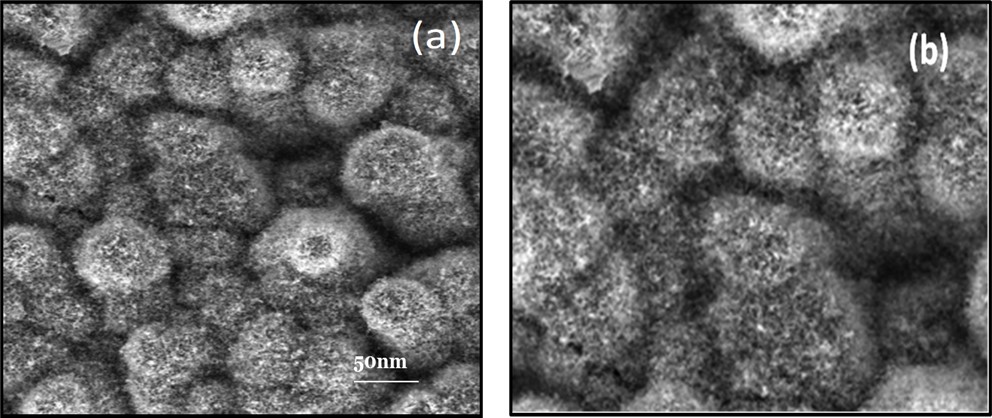
In Fig. 1, SEM images depict 2D-view of surface morphology of as-grown MWCNTs on ZnO catalyst at 600 °C. This micrograph gives the detail information of the size and density of CNTs. SEM images reveal that highly dense MWCNTs have been successfully synthesized on canonical nanocrystals of ZnO at silicon substrate. We draw the conclusion from Fig. 1(a) that ZnO catalyst are formed canonical nanocrystals and MWCNTs are synthesized on these canonical crystals with high density. The high magnification SEM image of as grown MWCNTs is shown in Fig 1 (b). Canonical structure of catalyst helps to increase the aspect ratio consequence of this performance parameters of sensors are increased in term of chemical reactivity, selectivity and sensitivity. It is also suggested from the morphological image of SEM that very high density of MWCNTs is occurred. High density of MWCNTs and high aspect ratio both are the prime factors for electronic based IOT sensors. In addition, high density increases the number of active sites for fast and stable detection of desired molecule.

jcm_10_1.jpgFigure 1 (a) SEM image of as-grown MWCNTs on ZnO catalyst (b) at high magnification
CNTs as electronic sensors for IOTs:

The term 'Internet of Things' (IoT) was coined in 1999 by Kevin Ashton. This is very innovative and first-hand term that relate the new concept of radio frequency identification (RFID) to provide the complete flow of information and also chain management [4]. In simple words, IoT refers to advance devices other than computers that are connected to the Internet and can send and receive information. IoTs is the notion of a ubiquitous computer environment in which custom-sized

electronics are effortlessly implanted into common things. Now a days, IoT is becoming a new paradigm that allows electrical gadgets and sensors to communicate with one another over the internet in order to improve our lives. This concept has broadened to include a diverse range of applications in fields such as healthcare, industries, agriculture and transportation. IoT uses smart devices and the internet to bring creative solutions to many corporate, governmental, and public/private enterprises throughout the world [5].

The development of IoT depend on the technological advancement of hardware to sense, read and process the information data to enhance the performance of devices. RFID technology and wireless sensor networks are examples of such advancement. Sensors is the key component of the IoT paradigm. However, the sensor hardware is the first step of the IoT network, but works as the nervous system of the IoT infrastructure.

jcm_10_3.jpg
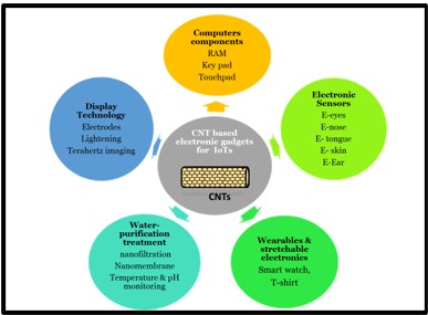
Figure 2: Diverse Applications of Carbon nanotubes for IoTs (Internet of Things)

Carbon nanotubes (CNTs) are a typical electrical substance that satisfy all of the desirable requirements for IoT sensor technologies. CNTs are carbon 1D allotropes with extraordinary electrical, mechanical, thermal and chemical properties which make them best candidate for the advanced electronic sensors for IoTs. Figure 2 shown the diverse application of CNTs as electronic gadgets for IoTs.

Conclusion

We have successfully grown high density of MWCNTs by CVD technique on ZnO catalyst for electronic sensor. For IoT-based


sensors with excellent performance, sensitivity, selectivity, and distance sensing, high MWCNT density is required. There is a growing need for new feasible manufacturing processes such as CVD that can shape carbon nanotubes in nanoscale devices while keeping great characteristics for sensors. It has diverse applications to develop the computer components, display device, wearable and stretchable sensors for medical uses, electronic sensors and water purification sensors for IoT platform. As a result of synthesised MWCNTs, this research would be beneficial for the next generation 5G communication and cloud computing boost to improve IoTs network.

Acknowledgment

Authors are thankful to Prof. Mohammad Zulfequar and Dr. Javid Ali, Department of Physics, Jamia Millia islamia, New Delhi for their suggestions and kind support to complete this research work.

References

1. Applications of Carbon Nanotubes in the Internet of Things Era Jinbo Pang, Alicja Bachmatiuk, Feng Yang, Hong Liu, Weijia Zhou, Mark H. Rümmel, Gianaurelio Cuniberti, Nano-Micro Lett. (2021) 13:191

2. Y. Saitoa, S. Uemurab “Field emission from carbon nanotubes and its application to electron sources,” Carbon, vol. 38, pp. 169-182, Feb. 2000.

3. H. Dai, J. H. Hafner, A.G. Rinzler, D.T.Colbert, R.E. Smalley, “Nanotubes as nanoprobes in scanning probe microscopy,” Nature, vol. 384, pp. 147-150, Nov. 1996.

4. J.A. Cardenas, J.B. Andrews, S.G. Noyce, A.D. Franklin, Carbon nanotube electronics for IoT sensors. Nano Futures 4(1), 012001 (2020). https:// doi. org/ 10. 1088/ 239.

5. E. Amram Bengio, D. Senic, L.W. Taylor, D.E. Tsentalovich, P. Chen et al., High efficiency carbon nanotube thread antennas. Appl. Phys. Lett. 111(16), 163109 (2017)

6. R. Seelaboyina, S. Boddepalli, K. Noh, M. Jeon, W. Choi, “Enhanced field emission from aligned multistage carbon nanotube emitter arrays,” Nanotechnology, vol. 19, pp. 065605-4, May. 2008.

7. A. C. Eletskii, “Carbon

nanotubes and their emission properties,” Phys.-Usp., vol. 45, pp. 369-402, April. 2002.

8. L. Wang, Z. Sun, T. Chen, W. Que, “Growth temperature effect on field emission properties of printable carbon nanotubes cathode,” Solid-State Electr., vol. 50, pp. 800-804, May. 2006.

9. S. Khan, Z. H. Khan, K.N. Tripathi, M. Husain, “Synthesis of carbon nanotubes using Ni95Ti5 nanocrystalline film as a catalyst,” J. Nanosci. Nanotechnol., vol. 7, pp. 1855-1859, June. 2007.

10. J. Ali, A. Kumar, S. Husain, M. Kumari, Harsh, M. Husain, “Characterization and field emission studies of uniformaly distributed multi-walled carbon nanotubes (MWMWCNTs) film grown by low pressure chemical vapour deposition (LPCVD),” Curr. Nanosci., vol. 7, pp. 333-336, June. 2011.

11. Z. H. Khan, S. Husain, M. Husain, “Variable range hopping in carbon nanotubes,” Curr. Nanosci., vol. 6, pp. 626-641, Dec. 2010.

12. S. Frank, P. Poncharal, Z. Wang, L. Walt, A. D. Heer, “Carbon nanotube quantum resistors.” Science., vol. 280, pp. 1744-1746, June. 1998.

13. V. Semet, V. T. Binh, P. Vincent, D. Guillot, K. B. K. Teo, M. Chhowalla, G. A.J. Amaratunga, W. I. Milne, P. Legagneux, D. Priba, “Field electron emission from individual carbon nanotubes of a vertically aligned array.” Appl. Phys. Lett., vol. 81, pp. 343-345, July. 2002.

14. J. F. AuBuchon, C. Daraio, L. H. Chen, A. I. Gapin, S. Jin, “Iron silicide root formation in carbon nanotubes grown by microwave PECVD”. J. Phys. Chem. B., vol. 109, pp. 24215-24219, Dec. 2005.

15. D. S. Chung, S. H. Park, H. W. Lee, J. H. Choi, S. N. Cha, J. W. Kim, J. E. Jang, K. W. Min, S. Cho, H. Yoon, M. J. Lee, J. S. Lee, C. K. Yoo, J. H. Kim, J. M. Jung, J. E. Y. W. Jin, Y. J. Park, J. B. You, “Carbon nanotube electron emitters with a gated structure using backside exposure processes,” Appl. Phys. Lett., vol. 80, pp. 4045-4047, May. 2002.

16. J. Ali, A. Kumar, S. Husain, M. Husain, “Effect of catalyst-deposition methods on the alignment of carbon nanotubes grown by low pressure chemical vapor deposition,” Nanosci. Nanotechnol. Lett., vol. 3, pp. 175-178, Aug. 2011.

17. S. Khan, K. N. Tripathi, M. Aggarwal, K. Tripathi, M. Husain, Z. H. Khan, “Field emission properties


of Fe70Pt30 catalysed multiwalled carbon nanotubes,” J. Exp. Nanosci., vol. 2, pp. 215-228. April. 2007.